- FIBER OPTIC TRANSCEIVERS >800G & 400G Transceivers >400G QSFP 112 FR4 2km Transceiver
400G QSFP 112 FR4 2km Transceiver
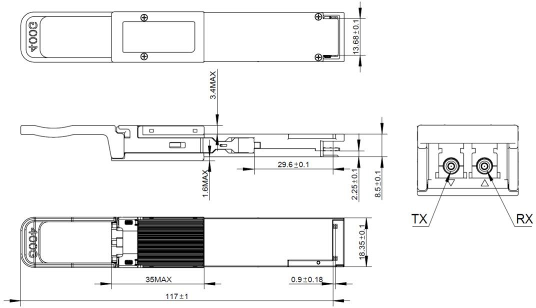
Ascent's Q112-400G-FR4-02 is a high-performance, hot-pluggable 400G QSFP112 optical transceiver designed for high-speed data center interconnects and 400G Ethernet applications over single-mode fiber. The module features four 106.25 Gb/s PAM4 optical lanes operating at CWDM wavelengths of 1271, 1291, 1311, and 1331 nm. An integrated optical multiplexer/demultiplexer enables transmission over duplex single-mode fiber with a reach of up to 2 km through a duplex LC interface. Designed for high-density networking environments, the transceiver supports a 4 × 106.25 Gb/s electrical interface, CMIS 5.2 management, and digital diagnostic monitoring. Its compact QSFP112 form factor and maximum power consumption of 9 W make it suitable for high-bandwidth switching and routing applications.
QSFP112 MSA compliant
4x106.25Gb/s PAM4 electrical interface
Maximum power consumption 9W@ Tcase = 70℃
Duplex LC connector
CWDM4 MUX/DEMUX design
Up to 2Km transmission on single mode fiber
Operating case temperature: 0℃~70℃
Single 3.3V power supply
RoHS-6 compliant
400G Ethernet
Data Center Applications
QSFP112 MSA Rev2.1
100G Lambda MSA
IEEE 802.3ck
CMIS Rev5.2
RoHS compliance
GR-468-CORE
Absolute Maximum Rating
Parameter | Symbol | Min | Typical | Max | Unit | Notes |
Storage Temperature | TSTG | -40 | 85 | ºC | ||
Operating Relative Humidity | RH | 5 | 85 | % | Note1 | |
Supply Voltage | VCC | -0.5 | 3.3 | 3.6 | V | |
Damage Threshold, each lane | PIN | 4.5 | dBm |
[1] Non-condensing.
Recommended Operating Condition
Parameter | Symbol | Min | Typical | Max | Unit | Notes |
Case temperature | Tcase | 0 | 70 | ℃ | ||
Supply Voltage | VCC | 3.135 | 3.3 | 3.465 | V | |
Supply Current | ICC | 2871 | mA | Tcase =70℃ | ||
Module Power Dissipation | P | 9 | W | Tcase =70℃ |
Transmitter Operating Characteristic-Optical,Electrica
Parameter | Symbol | Min | Typical | Max | Units | Notes |
Optical Data Rate, each Lane | 53.125±100ppm | GBd | ||||
Modulation Format | PAM4 | |||||
Line wavelengths |
| 1264.5 | 1271 | 1277.5 | nm | |
| 1284.5 | 1291 | 1297.5 | nm | ||
| 1304.5 | 1311 | 1317.5 | nm | ||
| 1324.5 | 1331 | 1337.5 | nm | ||
Total Average Launch Power | 9.3 | dBm | ||||
Average Launch Power, each lane | PAVG | -3.3 | 3.5 | dBm | ||
Optical Modulation Amplitude (OMA), each lane | OMA | -0.3 | 3.7 | dBm | ||
Extinction Ratio | ER | 3.5 | dB | |||
Side-Mode Suppression Ratio | SMSR | 30 | dB | |||
Launch power in OMA minus TDECQ, each lane, for ER≥4.5dB | -1.7 | dBm | ||||
Launch power in OMA minus TDECQ, each lane, for ER <4.5dB | -1.6 | dBm | ||||
Transmitter and Dispersion Eye Closure for PAM4, each Lane | TDECQ | 3.4 | dB | |||
Difference in Launch Power between any Two Lanes (OMAouter) | 4 | dB | ||||
Optical Return Loss Tolerance | 17.1 | dB | ||||
Transmitter Reflectance | -26 | dB | ||||
Average Launch Power of OFF Transmitter, each Lane | -20 | dBm | ||||
Electrical Data Rate, each lane | 53.125±100ppm | GBd | ||||
Differential pk-pk input Voltage tolerance | Vpp | 800 | mV | |||
DC Common Mode Voltage | Vcm | -350 | 2850 | mV | Note1 | |
Differential Termination Resistance Mismatch | -10 | 10 | % | |||
Effective return loss | 8.5 | dB | ||||
Differential to Common Mode Input Return Loss | IEEE 802.3ck Equation (120G-2) | dB | ||||
Module Stressed Input Test | IEEE 802.3ck 120G.3.4.2 | Note2 | ||||

[1] DC common mode voltage generated by the host. Specification includes effects of ground offset voltage.
[2] BER specified in IEEE 802.3ck 120G.1.1.
Receiver Operating Characteristic-Optical,Electrical
Parameter | Symbol | Min | Typical | Max | Units | Notes |
Optical Data Rate, each Lane | 53.125±100ppm | GBd | ||||
Modulation Format | PAM4 | |||||
Optical Input Power, each lane | 3.5 | dBm | ||||
Line wavelengths |
| 1264.5 | 1271 | 1277.5 | nm | |
| 1284.5 | 1291 | 1297.5 | nm | ||
| 1304.5 | 1311 | 1317.5 | nm | ||
| 1324.5 | 1331 | 1337.5 | nm | ||
Average receiver power, each lane | -7.3 | 3.5 | dBm | |||
Receiver power, each lane (OMA) | 3.7 | dBm | ||||
Difference in Receiver Power between any Two Lanes (OMA) | 4.1 | dB | ||||
Receiver Sensitivity (OMAouter) , each lane | max(-4.6, SECQ-6) | dBm | ||||
Stressed receiver sensitivity (OMAouter), each laned (max) | -2.6 | dBm | ||||
Receiver reflectance | -26 | dB | ||||
Electrical Data Rate, each lane | 53.125±100ppm | GBd | ||||
Differential Termination Resistance Mismatch | -10 | 10 | % | |||
Differential output Voltage pk-pk | Vpp |
845 | mV | |||
DC Common Mode Voltage | Vcm | -350 | 2850 | mV | Note 1 | |
Effective return loss | ERL | 8.5 | dB | |||
Transition time | 8.5 | ps | ||||
Common mode to differential return loss | IEEE 802.3ck Equation (120G-1) | dB | ||||
Note:
[1] DC common mode voltage generated by the host. Specification includes effects of ground offset voltage
Digital Diagnostic Function
Parameter | Symbol | Min | Typical | Max | Units | Notes |
Temperature monitor absolute error | DMI_Temp | -3 | 3 | ℃ | Note1 | |
Supply voltage monitor absolute error | DMI_Vcc | -5% | 5% | V | Note2 | |
Bias current monitor absolute error | DMI_Ibias | -10% | 10% | mA | ||
Laser power monitor absolute error | DMI_Tx | -3 | 3 | dB | ||
RX power monitor absolute error | DMI_Rx | -3 | 3 | dB |
[1] Temperature here is depending on module case around Max power dissipation. Temperature monitor is done over operating temperature.[2] Supply voltage monitor is done over operating voltage.
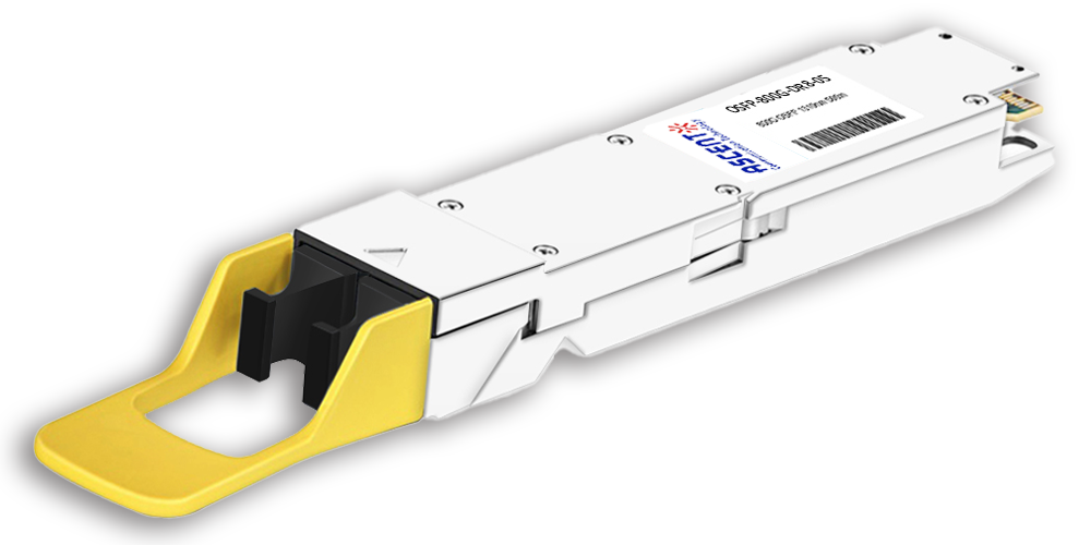
800G OSFP DR8 1310 nm 500 m
800 Gb/s DR8 OSFP 500m Optical Transceiver
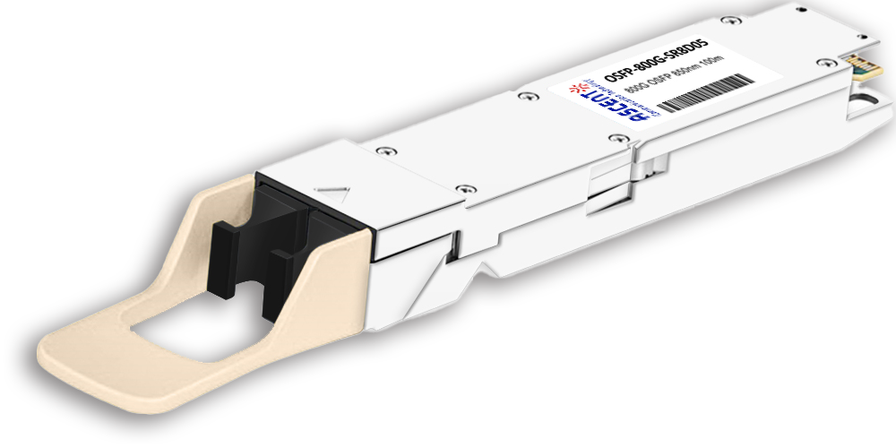
800G OSFP SR8 850 nm 100 m
OSFP-800G-SR8D-01 800 Gb/s OSFP SR8 850 nm 100 m Transceiver
400G QSFP56-DD 10km
400G QSFP-DD 4X100G LR1 Optical Transceiver
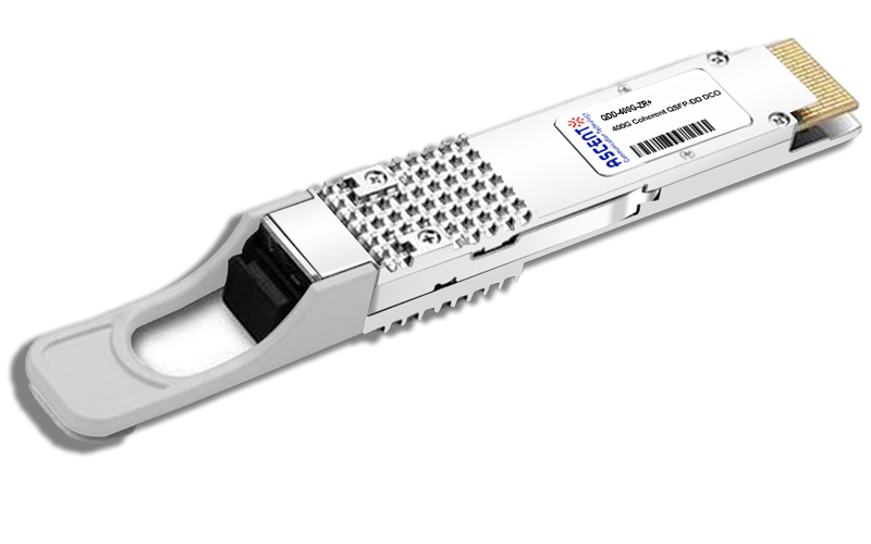
400G QSFP-DD ZR+
QSFP-DD-ZR-80 400 Gb/s QSFP-DD 80 km Transceiver
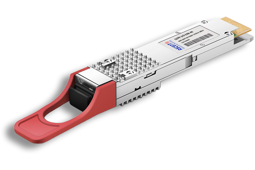
400G QSFP-DD ER8 40 km
QSFP-DD-ER8-40 400 Gb/s QSFP-DD 40 km Transceiver
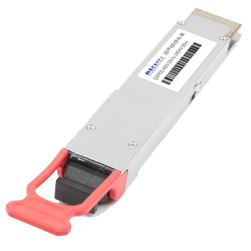
400G QSFP-DD 30 km
400 Gb/s QSFP-DD 30 km Transceiver
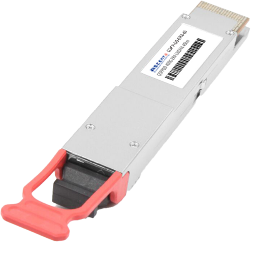
400G QSFP-DD 40 km
400 Gb/s QSFP-DD 40 km Transceiver
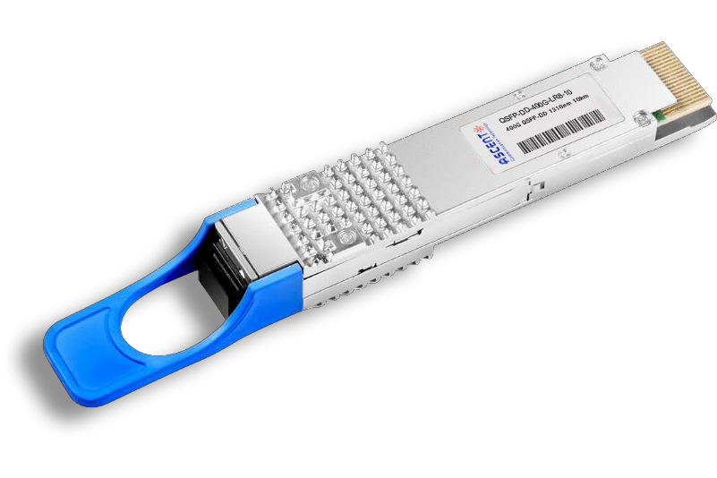
400G QSFP-DD LR8 1310 nm 10 km
QSFP-DD-LR8-10 400 Gb/s QSFP-DD LR8 10 km Transceiver

400G QSFP-DD LR4 CWDM 10 km
QSFP-DD-LR4-10 400 Gb/s QSFP-DD LR4 CWDM 10 km Transceiver
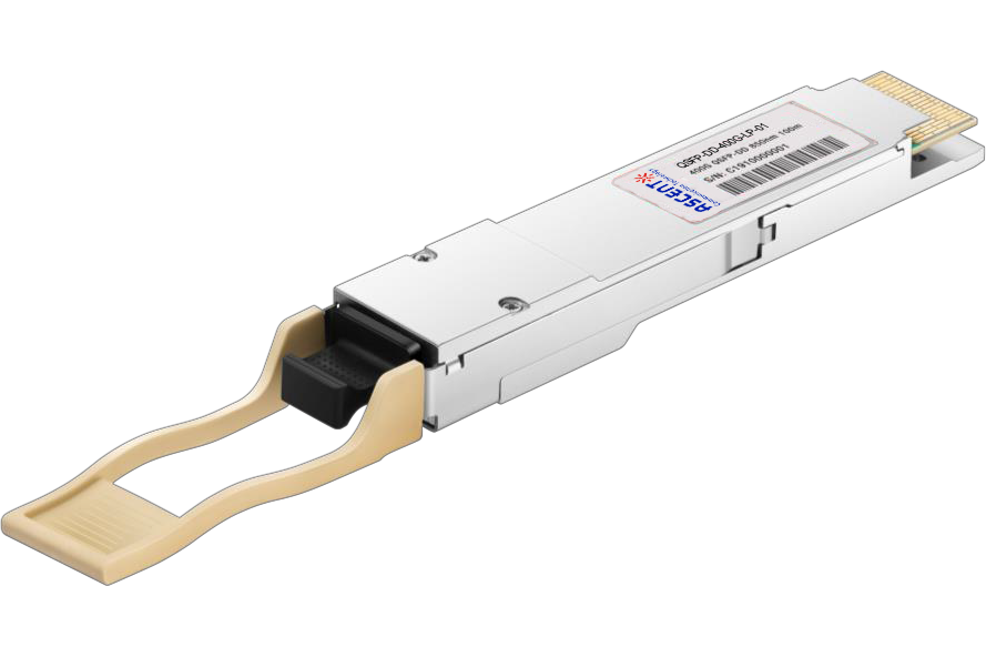
400G QSFP-DD SR8 850 nm 100 m
QSFP-DD-LP-01 400 Gb/s QSFP-DD SR8 100 m Transceiver
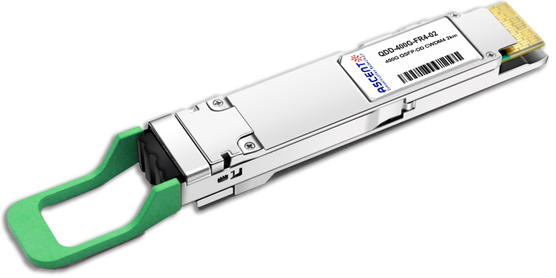
400G QSFP-DD FR4 2km
400 Gb/s QSFP-DD FR4 2 km DDM Transceiver
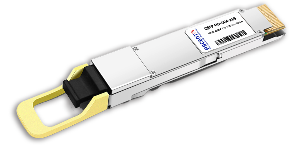
400G QSFP-DD DR4 500m
400 Gb/s QSFP-DD DR4 500m Transceiver
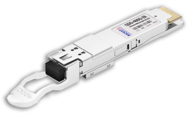
400G QSFP-DD DCO ZR
400G QSFP-DD DCO ZR Coherent Optical Transceiver
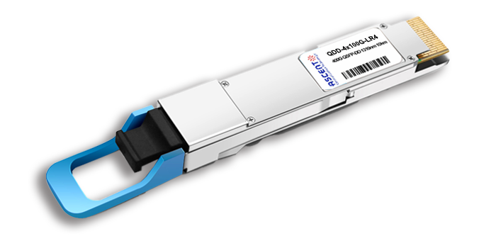
4X100G QSFP-DD LR4 10km
QDD 4x100G 1310nm LR 10 km Transceiver
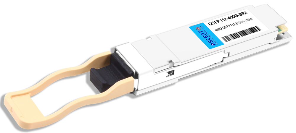
400G QSFP112 SR4 850 nm 100 m
QSFP112-400G-SR4-01 400 Gb/s QSFP112 SR4 850 nm 100 m Transceiver
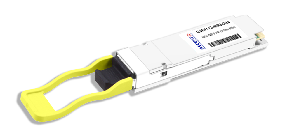
400G QSFP112 DR4 1310 nm 500 m
400G QSFP112 DR4 1310 nm Transceiver 500m
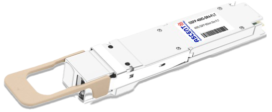
400G OSFP SR4 FLT 50m Transceiver
400 Gbps Multi-Mode 50m OSFP Transceiver
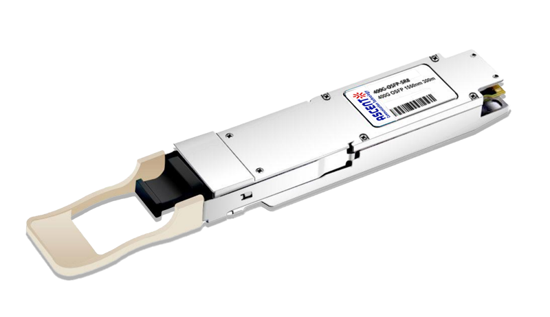
400G OSFP SR8 100m Transceiver
400 Gbps PSM8 Multi-Mode 100m OSFP Transceiver
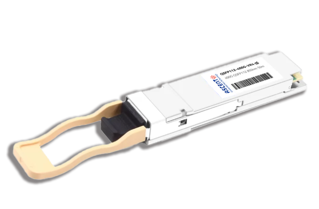
400G QSFP112 VR4 Transceiver
400G QSFP112 VR4
White Paper
Press Releases
Briefings 1
Briefings 2
Videos, etc.
QRG
Manual1
Manual2
Get in touch with our experts
Feedback