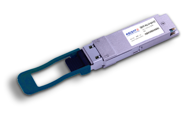
- FIBER OPTIC TRANSCEIVERS >40G & 25G Transceivers >40GBASE-UNIV QSFP+ MMF and SMF
40GBASE-UNIV QSFP+ MMF and SMF
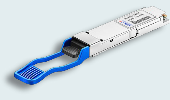
Ascentãs QSFP-AQ-LP-W4-02U is a transceiver module designed for 2 km (SMF) / 150 m (MMF) optical communication applications. They are compliant with the IEEE 802.3ba 40GBASE-LR4 standard referred to as LM4. The module converts 4 input channels (ch) of 10 Gb/s electrical data to 4 CWDM optical signals, and multiplexes them into a single channel for 40 Gb/s optical transmission. On the receiver side, the module optically de-multiplexes a 40 Gb/s input into 4 CWDM channel signals, and converts them into 4 channels of output electrical data.
ã Hot-pluggable QSFP+ form factor
ã Operates over duplex multi-mode and single-mode fiber with dual LC receptacles
ã Supports 41.2 Gbs/ aggregate bit rate
ã Up to 2 km transmission distance over SMF
ã Up to 150 m transmission distance on OM3
ã Hot-pluggable QSFP+ form factor
ã Uncooled 4x 10 Gb/s CWDM transmitter
ã XLPPI electrical interface
ã Built-in digital diagnostic functions, including Tx/Rx power monitoring
ã Case operating temperature range: 0 ô¯C to +70 ô¯C
ã Power dissipation < 3.5 W
ã Compliant with IEEE 802.3ba
ã RoHS compliant
General Product Characteristics
Item | Value | Notes |
Module Form Factor | QSFP+ | |
Maximum Aggregate Data Rate | 41.2 Gb/s | |
Maximum Data Rate per Lane | 10.3125 Gb/s | |
Protocols Supported | 40G Ethernet | |
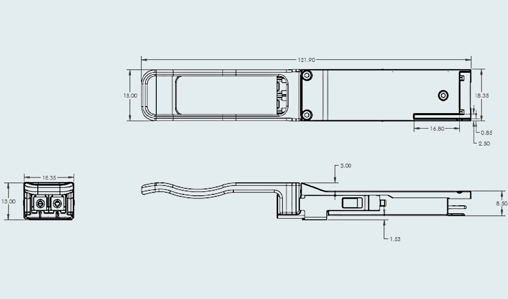
Electrical Interface and Pinãout | 38ãpin edge connector | Pinãout as defined by the QSFP+ MSA |
Maximum Power Consumption | 3.5 W | |
Management Interface | Serial, I2Cãbased, 400 kHz maximum frequency | As defined by the QSFP+ MSA |
Data Rate Specifications
Item | Symbol | Min. | Typ. | Max. | Unit | Note |
Bit Rate per Lane | BR | 10.313 | Gb/sec | 1 | ||
Bit Error Ratio | BER | 10ã12 | 2 | |||
Link Distance on OM3 | d | 150 | m | |||
Link Distance on OM4 | d | 160 | m | |||
Link Distance on SMF | d | 2000 | m |
Notes:
1. Adapted from 40GBASEãLR4, IEEE 802.3ba
2. Tested with a PRBS 231ã1 test pattern.
Absolute Maximum Ratings
Item | Symbol | Min. | Typ. | Max. | Unit | Notes |
Maximum Supply Voltage | Vcc1, VccTx, VccRx | ã0.5 | 4 | V | ||
Storage Temperature | Ts | ã40 | 85 | ô¯C | ||
Case Operating Temperature | Top | 0 | 70 | ô¯C | ||
Relative Humidity | RH | 0 | 85 | % | Nonãcondensing | |
Damage Threshold, per Lane | DT | 3.4 | dBm |
Electrical Characteristics (TOP = 0 ô¯C to 70ô¯C, VCC = 3.1 V to 3.47 V)
Item | Symbol | Min. | Typ. | Max. | Unit | Notes |
Supply Voltage | Vcc1, VccTx, VccRx | 3.1 | 3.47 | V | ||
Supply Current | Icc | 1.13 | A | |||
Transmit TurnãOn Time | 2000 | ms | 1 | |||
Transmitter (per Lane) | ||||||
SingleãEnded Input Voltage Tolerance | VinT | ã0.3 | 4.0 | V | ||
Differential Data Input Swing | Vin,pp | 120 | 1200 | mVpp | 2 | |
Differential Input Threshold | 50 | mV | ||||
AC Common Mode Input Voltage Tolerance (RMS) | 15 | mV | ||||
Differential Input Return Loss | Per IEEE P802.3ba, Section 86A.4.1.1 | dB | 3 | |||
J2 Jitter Tolerance | Jt2 | 0.17 | UI | |||
J9 Jitter Tolerance | Jt9 | 0.29 | UI | |||
Data Dependent Pulse Width Shrinkage | DDPWS | 0.07 | UI | |||
Eye Mask Coordinates {X1, X2, Y1, Y2} | 0.11, 0.31, 95, 350 | UI mV | 4 | |||
Receiver (per Lane) | ||||||
SingleãEnded Output Voltage | ã0.3 | 4.0 | V | |||
Differential Data Output Swing | Vout,pp | 0 | 800 | mVpp | 5 | |
AC Common Mode Output Voltage (RMS) | 7.5 | mV | ||||
Termination Mismatch at 1 MHx | 5 | % | ||||
Differential Output Return Loss | Per IEEE P802.3ba, Section 86A.4.2.1 | dB | 3 | |||
Common Mode Output Return Loss | Per IEEE P802.3ba, Section 86A.4.2.2 | dB | 3 | |||
Output Transition Time, 20% To 80% | 28 | ps | ||||
J2 Jitter Output | Jo2 | 0.42 | UI | |||
J9 Jitter Output | Jo9 | 0.65 | UI | |||
Eye Mask Coordinates #1 {X1, X2, Y1, Y2} | 0.29, 0.5 150, 425 | UI mV | 4 | |||
Power Supply Ripple Tolerance | PSR | 50 | mVpp | |||
Notes:
1. From powerãon and end of any fault conditions.
2. After internal AC coupling. Selfãbiasing 100 ãÎ differential input.
3. 10 MHz to 11.1 GHz range
4. Hit ratio = 5 x 10ã5
5. AC coupled with 100 ãÎ differential output impedance.
Optical Characteristics (TOP = 0 to 70ô¯C, VCC = 3.1 to 3.47 V)
Item | Symbol | Min. | Typ. | Max. | Unit | Notes |
Transmitter (per Lane) | ||||||
Signaling Speed per Lane | 11.2 | GBd | 1 | |||
Lane Center Wavelengths (Range) | 1264.5ã1277.5 1284.5ã1297.5 1304.5ã1317.5 1324.5ã1337.5 | nm | ||||
Total Average Launch Power | Pout | 8.3 | dBm | |||
Average Launch Power per Lane, MMF | TXPx | ã7.0 | 4.3 | dBm | ||
Average Launch Power per Lane, SMF | TXPx | ã10.0 | 2.3 | dBm | 2 | |
Transmit OMA per Lane, MMF | TxOMA | ã3.0 | 4.8 | dBm | ||
Transmit OMA per Lane, SMF | TxOMA | ã6.0 | 3.5 | dBm | 3 | |
Transmitter Dispersion Penalty, MMF | TXPãTDP | 4.7 | dBm | |||
Transmitter Dispersion Penalty, SMF | TXPãTDP | 2.6 | dBm | |||
Average Launch Power of OFF Transmitter, per Lane | ã30 | dBm | ||||
Relative Intensity Noise | RIN | ã128 | dB/Hz | 4 | ||
Sidemode Suppression Ratio | SSRmin | 30 | dB | |||
Optical Extinction Ratio | ER | 3.5 | dB | |||
Optical Return Loss Tolerance | 20 | dB | ||||
Transmitter Reflectance | ã12 | dB | ||||
Transmitter Eye Mask Definition {X1, X2, X3, Y1, Y2, Y3} | (0.25, 0.4, 0.45, 0.25, 0.28, 0.4) | |||||
Jitter Generation | Per OTL3.4 section 4.14.1 | |||||
Receiver (per Lane) | ||||||
Signaling Speed per Lane | 11.2 | GBd | 5 | |||
Lane Center Wavelengths (Range) | 1264.5ã1277.5 1284.5ã1297.5 1304.5ã1317.5 1324.5ã1337.5 | nm | ||||
Receive Power (OMA) per Lane, MMF | RxOMA | 4.8 | dBm | |||
Receive Power (OMA) per Lane, SMF | RxOMA | 3.3 | dBm | |||
Damage Threshold per Lane | PMAX | 5.5 | dBm | |||
Average Receive Power per Lane, MMF | RXPx | ã10.0 | 4.3 | dBm | ||
Average Receive Power per Lane, SMF | RXPx | ã13.7 | 2.3 | dBm | 6 | |
Receiver Sensitivity (OMA) per Lane, MMF | Rxsens | ã10.5 | dBm | |||
Receiver Sensitivity (OMA) per Lane, SMF | Rxsens | ã10.5 | dBm | 7 | ||
Stressed Receiver Sensitivity (OMA) per Lane, MMF | SRS | ã5.0 | dBm | |||
Stressed Receiver Sensitivity (OMA) per Lane, SMF | SRS | ã8.5 | dBm | |||
Return Loss | RL | ã20 | dB | |||
Vertical Eye Closure Penalty, per Lane | 3.6 | dB | ||||
Receive Electrical 3 Db Upper Cutoff Frequency, per Lane | 12.3 | GHz | ||||
LOS DeãAssert | LOSD | ã12 | dBm | 8 | ||
LOS Assert | LOSA | ã28 | dBm | 8 | ||
LOS Hysteresis | 1 | dB | ||||
Notes:
1. Transmitter consists of 4 lasers operating at 10.3 Gb/s each.
2. Minimum value is informative.
3. Even if TDP < 0.5 dB (MMF) or TDP < 0.8 dB (SMF), TxP ã TDP must be greater than this value.
4. RIN is scaled by 10 * log(10/4) to maintain SNR outside of transmitter.
5. Receiver consists of 4 photodetectors operating at up to 10.3 Gb/s each.
6. Minimum value is informative, equals min. TxOMA with infinite ER and max. channel insertion loss.
7. SMF receiver sensitivity guaranteed by design, but not measured in production.
8. LOS Assert and DeãAssert values are informative and may vary between MMF and SMF uses.


64G SFP56 850nm 100m
64 Gb/s SFP56 SW Fibre Channel 850nm Transceiver
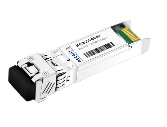
40/100G SFP28 SWDM4 100m
40/100Gb/s QSFP28, Bi-Di, Duplex LC 100m Transceiver

40G QSFP+ ER4 Industrial 40 km
40 Gb/s QSFP+ ER4 40 km Transceiver

40G QSFP+ ER4 40 km
40 Gb/s QSFP+ ER4 40 km Transceiver

40G QSFP+ LR4 Industrial 10 km
40 Gb/s QSFP+ LR4 10 km Transceiver

40G QSFP+ LR4 10 km
QSFP-AQ-LP-W4-10 40 Gb/s QSFP LR4 10 km Transceiver

40G QSFP+ PSM4 2 km
40 Gb/s QSFP+ PSM4 Transceiver 2km
40G QSFP+ PLR4 1310 nm 10 km
QSFP-AQ-MP-31-10 40 Gb/s QSFP+ PSM 1310nm 10km MPO Optical Transceiver

40G QSFP+ CSR4 300m
40 Gb/s 300m QSFP+ CSR4 Transceiver
40G QSFP+ CWDM 2 km
40G QSFP+ CWDM 2 km
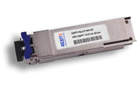
40G QSFP CWDM 20 km
QSFP-AQ-LP-W4-20 40 Gb/s QSFP CWDM 20 km Transceiver
40G QSFP+ SR4 300 m
40 Gb/s QSFP+ SR4 Transceiver with DDM
40G QSFP+ BIDI 150m
40 Gb/s QSFP+ BiDi Transceiver 150m
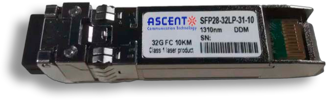
32G SFP28 1310 nm 10 km
32G FC 1310 nm 10 km SFP28 Transceiver

32G SFP28 SR 850 nm 100 m
SFP28-32LP-85-01 32GBASE-SR SFP28 850 nm 100 m DOM Transceiver
25G SFP28 BIDI 80 km
25G SFP28 BIDI 80 km Transceiver
.png)
25G SFP28 CWDM 10 km(E)
25 Gb/s CWDM EML SFP28 10 km Transceiver
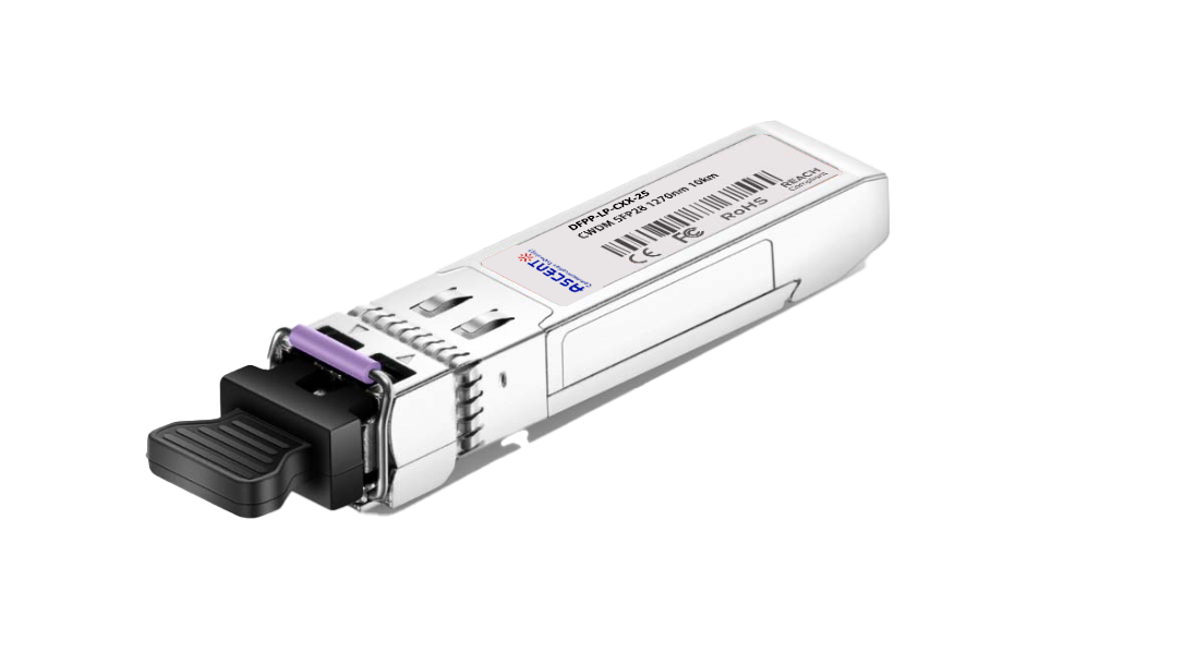
25G SFP28 CWDM 10 km(D)
25 Gb/s CWDM SFP28 10 km Transceiver
25G SFP28 ZR 1310nm 80km
25 Gbps 1310 nm 80 km SFP28 ZR Transceiver
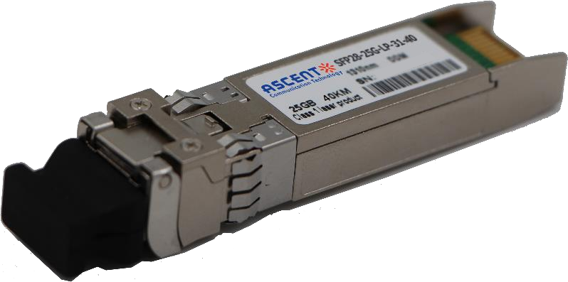
25G SFP28 1310 nm 40km
25 Gb/s 1310 nm Single-Mode SFP28 Transceiver
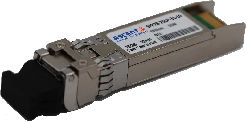
25G SFP28 1310 nm 10 km
SFP28-25LP-31-10 25 Gb/s 1310 nm Single-Mode SFP+ Transceiver
25G SFP28 850 nm 300m
25 Gb/s 850 nm Multi-Mode SFP28 300m Transceiver
25G SFP28 850 nm 100m
SFP28-25LP-85-01 28 Gb/s 850 nm Multi-Mode SFP28 Transceiver

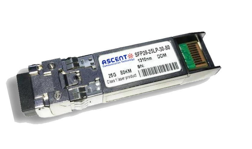
10/25G SFP28 1310nm 40km
10/25 Gb/s SFP28 1310 nm 40km Transceiver
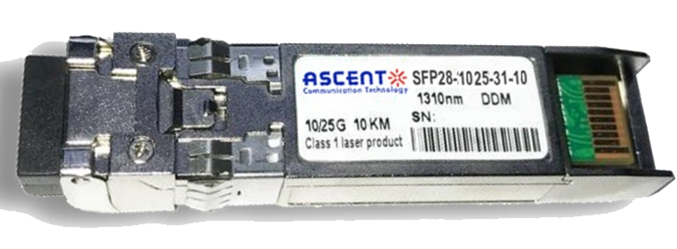
10/25G SFP28 1310nm 10km
10/25 Gb/s SFP28 1310 nm 10km DDM Transceiver

10/25G SFP28 850 nm 300m
10/25 Gb/s SFP28 850 nm 300m Transceiver

10/25G SFP28 850 nm 100m
10/25 Gb/s SFP28 850 nm 100m Transceiver
White Paper
Press Releases
Briefings 1
Briefings 2
Videos, etc.
QRG
Manual1
Manual2
Get in touch with our experts
Feedback