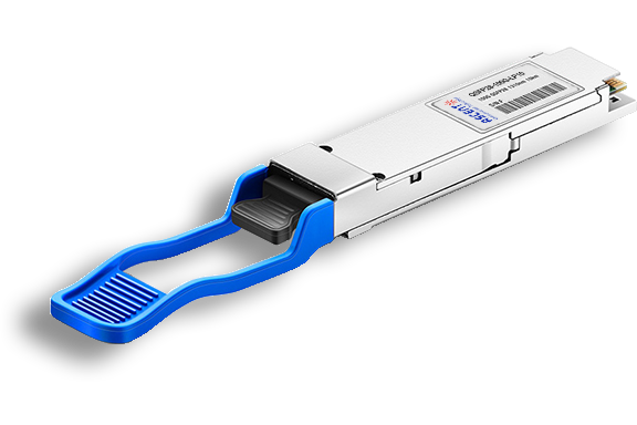
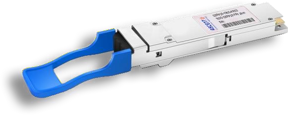
- FIBER OPTIC TRANSCEIVERS >200G & 100G Transceivers >100G QSFP28 CWDM4 1310 nm 2 km
.png)
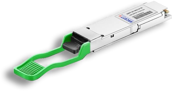
100G QSFP28 CWDM4 1310 nm 2 km
Ascentãs QSFP28-100G-LP02 transceiver modules are designed for use in 100 Gigabit Ethernet links over single mode fiber. They are compliant with the QSFP28 MSA, CWDM4 MSA, IEEE 802.3ba and IEEE 802.3bm. They are suitable to be used in various applications, such as data centers, high-performance computing networks, enterprise core and distribution layer applications. The central wavelengths of the 4 CWDM channels are 1271, 1291, 1311 and 1331 nm. It contains a duplex LC connector for the optical interface and a 38-pin connector for the electrical interface. This product converts the 4- channel 25Gb/s electrical input data into CWDM optical signals (light), by a 4-wavelength Distributed Feedback Laser (DFB) TO. The 4 wavelengths are multiplexed into a single 100Gb/s data, propagating out of the transmitter module via the SMF. The receiver module accepts the 100Gb/s optical signals input, and de-multiplexes it into 4 CWDM 25Gb/s channels. Each wavelength light is collected by a discrete photo diode, and then outputted as electric data after amplified by a TIA. The product is designed with form factor, optical/electrical connection and digital diagnostic interface according to the QSFP28 Multi-Source Agreement (MSA). The optical transceiver is compliant per the RoHS Directive 2011/65/EU.
ã Supports 103.1Gb/s aggregate bit rate
ã 4x25Gb/s electrical interface
ã 4X25Gb/s CWDM transmitter and PIN/TIA receiver
ã Maximum link length of 2km on Single Mode Fiber (SMF)
ã Hot-pluggable QSFP28 from factor
ã Single 3.3V power supply
ã Integrated 4-channel CWDM mux/Demux for duplex LC operation
ã Duplex LC receptacles
ã Maximum power dissipation<3.5W
ã RoHS-6 compliant and lead-free
ã I2C management interface
ã Commercial operating temperature: 0ô¯C to +70ô¯C
Absolute Maximum Ratings
Parameter | Symbol | Min. | Typ. | Max. | Unit | Note |
Storage Temperature | Ts | -40 | -- | 85 | ô¯C | |
Storage Ambient Relative Humidity | HA | 0 | -- | 85 | % | |
Maximum Supply Voltage | VCC | -0.5 | -- | 3.6 | V | |
Lead Soldering Temperature/Time | TSOLD | -- | -- | 260/10 | ô¯C /sec | 1 |
Lead Soldering Temperature/Time | TSOLD | -- | -- | 360/10 | ô¯C /sec | 2 |
1. Suitable for wave soldering.
2. Only for soldering by iron.
Optical Characteristics
Parameter Transmitter(per lane) | Symbol | Min. | Typ. | Max. | Unit | Note |
Signaling Speed per Lane | 25.78125 ôÝ 100 ppm | Gb/s | 1 | |||
Center Wavelength | ö£C | -- | 1264.5 ~ 1277.5 1284.5 ~ 1297.5 1304.5 ~ 1317.5 1324.5 ~ 1337.5 | -- | nm | |
Extinction Ratio | ER | 3.5 | -- | -- | dB | |
Side Mode Suppression Ratio | SMSR | 30 | -- | -- | dB | |
Total Average Launch Power | Ptot | -- | -- | 8.5 | dBm | |
Average Launch Power, Each Lane | Po | -6.5 | -- | 2.5 | dBm | |
OMA, Each Lane | OMA | -4 | -- | 2.5 | dBm | CW,ER>3.5dB |
Difference in Launch Power between Any Two Lanes (OMA) | 5 | dB | ||||
TDP, Each Lane | TDP | 3.0 | dB | 2 | ||
Average Launch Power of OFF Transmitter, Each Lane | Poff |
-30 |
dBm | |||
Transmitter Eye Mask Definition {X1,X2,X3,Y1,Y2,Y3} | {0.31, 0.40, 0.45, 0.34, 0.38, 0.4} | 3 | ||||
Receiver(per lane) | ||||||
Signaling Speed per Lane | 25.78125 ôÝ 100 ppm | Gb/s | 4 | |||
Input Optical Wavelength | ö£IN | 1264.5 ~ 1277.5 1284.5 ~ 1297.5 1304.5 ~ 1317.5 1324.5 ~ 1337.5 | nm | |||
Damage Threshold | 3.5 | dBm | ||||
Receiver Power (OMA), Each Lane | 2.5 | dBm | ||||
Rx Sensitivity(OMA) per Lane | RSENS | -10 | dBm | 5 | ||
Stressed Receiver Sensitivity (OMA), Each Lane | SRS | -7.3 | dBm | 6 | ||
Conditions of stressed receiver sensitivity test | ||||||
Vertical Eye Closure Penalty, Each Lane | VECP | 1.9 | dB | |||
Stressed Eye J2 Jitter, Each Lane | J2 | 0.33 | UI | |||
Stressed Eye J4 Jitter, Each Lane | J4 | 0.48 | UI | |||
SRS Eye Mask Definition {X1, X2, X3, Y1, Y2, Y3} | {0.39, 0.50, 0.50, 0.39, 0.39, 0.4} | |||||
Loss of Signal Assert | PA | -24 | -13.6 | dBm | ||
Loss of Signal De-assert | PD | -11.6 | dBm | |||
LOS Hysteresis | PD - PA | 0.5 | 6 | dB | ||
1. Transmitter consists of 4 lasers operating at 25.78 Gb/s each.
2. TDP value does not include MPI penalty.
3. Hit ratio of 5x10⁻⁵, per IEEE.
4. Receiver consists of 4 photodetectors operating at 25.78 Gb/s each.
5. Sensitivity is specified at 5x10⁻⁵ BER.
6. Measured with CWDM4 MSA2 conformance test signal at TP3 for 5x10⁻⁵ BER.
Electrical Interface Characteristics
Parameter | Symbol | Min. | Typ. | Max. | Unit | Note |
Supply Voltage | VCC | 3.135 | 3.465 | V | ||
Supply Current | ICC | 1.12 | A | |||
Module Total Power | P | 3.5 | W | 1 | ||
Transmitter | ||||||
Signaling Rate per Lane | 25.78125ôÝ100ppm | Gb/s | ||||
Differential Data Input Swing per Lane | Vin, pp | 900 | mV | |||
Differential Input Return Loss(min) | RLd(f) | 9.5 ã 0.37f, 0.01ãÊf<8 4.75-7.4log10(f/14), 8ãÊf<19 | dB | |||
Differential to Common Mode Input Return Loss(min) | RLdc(f) | 22-20(f/25.78), 0.01ãÊf<12.89 15-6(f/25.78), 12.89ãÊf<19 | dB | |||
Differential Termination Mismatch | 10 | % | ||||
Eye Width | 0.46 | UI | ||||
Applied Pk-Pk Sinusoidal Jitter | Per IEEE802.3bm Table 88-13 | -- | ||||
Eye Height | 95 | mV | ||||
Receiver | ||||||
Signaling Rate per Lane | 25.78125ôÝ100ppm | Gb/s | ||||
Differential Data Output Wwing | Vout, pp | 100 | 400 | mVpp | 2 | |
300 | 600 | |||||
400 | 600 | 800 | ||||
600 | 1200 | |||||
Eye Width | 0.57 | UI | ||||
Vertical Eye Closure | VEC | 5.5 | dB | |||
Differential Output Return Loss (min) | RLd(f) | 9.5-0.37f, 0.01ãÊf<8 4.75-7.4log10(f/14), 8ãÊf<19 | dB | |||
Common to Differential Mode Conversion Return Loss (min) | RLdc(f) | 22-20(f/25.78), 0.01ãÊf<12.89 15-6(f/25.78), 12.89ãÊf<19 | dB | |||
Differential Termination Mismatch | 10 | % | ||||
1. Maximum total power value is specified across the full temperature and voltage range.
2. Output voltage is settable in 4 discrete range via I2C.Default range is Range 2 (400 ã 800mV).
Digital Diagnostic Functions
Ascentãs QSFP28-100G-LP02 supports transceivers support the I2C-based diagnostics interface specified by the QSFP28 MSA Transceiver temperature.

200G QSFP DD LR4 10km
200 Gb/s QSFP DD LR4 10 km Transceiver
200G QSFP56 SR4 850 nm 100 m
QSFP56-200G-SR01 200 Gb/s QSFP56 SR4 850 nm 100 m Transceiver

100G QSFP28 LX4 2km
100 Gb/s 2km QSFP28 LX4 Transceiver

100G QSFP28OA LR4 10km
100 Gb/s 10 km QSFP28 LR4 Transceiver

100G QSFP28 ZR4 1310 nm 80 km
QSFP28-100G-LP80 QSFP28 100 Gbps ZR4 Transceiver
100G QSFP28 ER4L 1310 nm 40 km
QSFP28-100G-LP40 100 Gb/s 40 km QSFP28 ER4 Lite Transceiver

100G QSFP28 ER4 1310 nm 40 km
100 Gb/s 40 km QSFP28 ER4 Transceiver
100G QSFP28 LR4 1310 nm 10 km
QSFP28-100G-LP10 100 Gb/s 10km QSFP28 LR4 Transceiver
100G QSFP28 LR Single ö£ 10 km
100G QSFP28 LR1 10 km Single Channel

100G QSFP28 DR Single ö£ 500 m
QSFP28 100G DR Single Lambda Transceiver
100G QSFP28 PSM4 1310 nm 2 km
QSFP28-100G-PSM4 100 Gb/s 1310 nm 2 km Transceiver
100G QSFP28 SR4 850 nm 100 m
QSFP28-100G-SR01 100 Gb/s SR4 850 nm 100 m Transceiver
100G QSFP28 FR Single ö£ 1310 nm 2 km
100G QSFP28 FR 2km Transceiver

100G QSFP28 SR01 BIDI MMF 850nm 100m
QSFP28 BIDI 100 Gb/s SR Transceiver 100m

100G QSFP28 BIDI 80km
QSFP28 BIDI 100 Gb/s ZR4 Transceiver 80km

100G QSFP28 BIDI 40km
QSFP28 BIDI 100 Gb/s ER Transceiver 40km

100G QSFP28 EZR4 100km
QSFP28 100Gb/s EZR4 Transceiver 100km

100G SFP56 ER1 30km
SFP56-DD 100G-ER1 Optical Transceiver 30km

100G SFP56 LR1 10km
SFP56-DD 100G-LR1 Optical Transceiver 10km
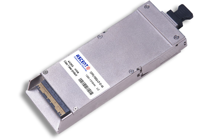
100G CFP2 ER4 40 km
CFP2-LP-31-40 100 Gb/s CFP2 ER4 40 km Transceiver
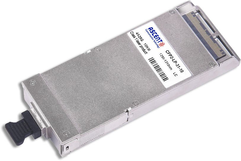
100G CFP2 LR4 10 km
CFP2-LP-31-10 100 Gb/s CFP2 LR4 10 km Transceiver
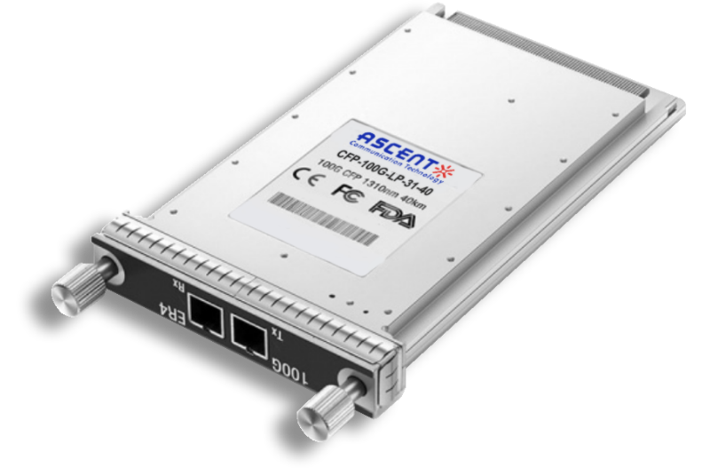
100G CFP ER4 40 km
CFP-LP-31-40 100 Gb/s CFP ER4 40 km Transceiver
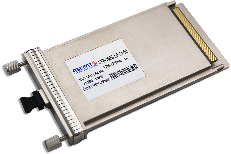
100G CFP LR4 10 km
CFP-LP-31-10 100 Gb/s CFP LR4 10 km Transceiver
White Paper
Press Releases
Briefings 1
Briefings 2
Videos, etc.
QRG
Manual1
Manual2
Get in touch with our experts
Feedback