- FIBER OPTIC TRANSCEIVERS >800G & 400G Transceivers >400G QSFP-DD FR4 2km
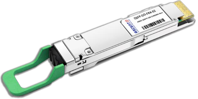
400G QSFP-DD FR4 2km
Ascentãs QSFP-DD-FR4-02 is a 400 Gb/s Quad Small Form Factor Pluggable-double density (QSFP-DD) optical module designed for 2km optical communication applications. The module converts 8 channels of 50 Gb/s (PAM4) electrical input data to 4 channels of CWDM optical signals, and multiplexes them into a single channel for 400Gb/s optical transmission. Reversely, on the receiver side, the module optically de-multiplexes a 400Gb/s optical input into 4 channels of CWDM optical signals, and converts them to 8 channels of 50 Gb/s (PAM4) electrical output data. The central wavelengths of the 4 CWDM channels are 1271, 1291, 1311 and 1331 nm as members of the CWDM wavelength grid defined in ITU-T G.694.2. It contains a duplex LC connector for the optical interface and a 76-pin connector for the electrical interface. To minimize the optical dispersion in the long-haul system, single-mode fiber (SMF) has to be applied in this module. Host FEC is required to support up to 2 km fiber transmission QSFP-DD-FR2-02 is designed with form factor, optical/electrical connection and digital diagnostic interface according to the QSFP-DD Multi- Source Agreement (MSA) Type 2. It has been designed to meet the harshest external operating conditions including temperature, humidity and EMI interference.
ôñ Compliant with 400G-FR4 Technical Specification rev 2.0 (100G Lambda MSA) and 400GBASE-FR4(IEEE802.3cu)
ôñ Compliant with IEEE 802.3bs standard: 400GAUI-8 electrical interface
ôñ Compliant with QSFP-DD MSA HW Rev 5.0; type 2 housing with duplex LC connector
ôñ Compliant with QSFP-DD CMIS Rev 4.0
ôñ Maximum power consumption 12 W
ôñ Case operating temperature 0ô¯C to 70ô¯C
ôñ Two wire serial Interface with digital diagnostic monitoring
ôñ Complies with EU Directive 2011/65/EU (RoHS compliant)
ôñ Class 1 Laser
Absolute Maximum Ratings
Parameter | Symbol | Min. | Max. | Unit | Note |
Storage Temperature | TS | -40 | 85 | ô¯C | |
Supply Voltage | VCC | -0.5 | 3.6 | V | |
Relative Humidity (non-condensing) | RH | 5 | 95 | % | Non-condensing |
Data Input Voltage Differential | lVDIP-VDINl | - | 1 | V | |
Control Input Voltage | VI | -0.3 | VCC+0.5 | V | |
Control Output Voltage | VI | -20 | 20 | V |
Recommended Operating Conditions
Parameter | Symbol | Min. | Typ. | Max. | Unit | Note |
Operating Case Temperature | TOPR | 0 | - | 70 | ô¯C | |
Power Supply Voltage | VCC | 3.135 | 3.3 | 3.465 | V | |
Instantaneous Peak Current at Hot Plug | ICC_IP | - | - | 4800 | mA | |
Sustained Peak Current at Hot Plug | ICC_SP | - | - | 3960 | mA | |
Maximum Power Dissipation | PD | - | - | 12 | W | |
Maximum Power Dissipation, Low Power Mode | PDLP | - | - | 1.5 | W | |
Signaling Rate per Lane | SRL | - | 53.125 | - | GBd | 1 |
Two Wire Serial Interface Clock Rate | - | - | - | 400 | kHz | |
Power Supply Noise Tolerance | - | - | - | 66 | mV | 2 |
Rx Differential Data Output Load | - | - | 100 | - | öˋ | |
Operating Distance | - | 2 | - | 2000 | m |
Notes:
1. PAM4
2. 10 Hz to 10 MHz
Electrical Specification High Speed Signal (compliant with IEEE 802.3bs 400GAUI-8)
Parameter | Symbol | Min. | Typ. | Max. | Unit | Notes |
Receiver (Module Output) | ||||||
AC Common-Mode Output Voltage (RMS) | - | - | 17.5 | mV | ||
Differential Output Voltage | - | - | 900 | mV | ||
Near-End Eye Height, Differential | 70 | - | - | mV | ||
Far-End Eye Height, Differential | 30 | - | - | mV | ||
Far End Pre-Cursor Ratio | -4.5 | - | 2.5 | % | ||
Differential Termination Mismatch | - | - | 10 | % | ||
Transition Time (Min., 20% To 80%) | 9.5 | - | - | ps | ||
DC Common Mode Voltage | -350 | - | 2850 | mV | ||
Transmitter (Module Input) | ||||||
Differential pk-pk Input Voltage Tolerance | 900 | - | - | mV | ||
Differential Termination Mismatch | - | - | 10 | % | ||
Single-Ended Voltage Tolerance Range | -0.4 | - | 3.3 | V | ||
DC Common Mode Voltage | -350 | - | 2850 | mV | ||
Electrical Specification Low Speed Signal (compliant with QSFP-DD HW Rev 5.0)
Parameter | Symbol | Min. | Max. | Unit | Note |
Module Output SCL and SDA | VOL | 0 | 0.4 | V | |
Module Input SCL and SDA | VIL | -0.3 | VCC*0.3 | V | |
VIH | VCC*0.7 | VCC+0.5 | V | ||
InitMode, ResetL, and ModSelL | VIL | -0.3 | 0.8 | V | |
VIH | 2 | VCC+0.3 | V | ||
IntL | VOL | 0 | 0.4 | V | |
VOH | VCC-0.5 | VCC+0.3 | V |
Optical Characteristics
Parameter | Symbol | Min. | Typ. | Max. | Unit | Note | |
Transmitter | |||||||
Wavelength L0 | ö£C0 | 1264.5 | 1271 | 1277.5 | nm | ||
Wavelength L1 | ö£C1 | 1284.5 | 1291 | 1297.5 | nm | ||
Wavelength L2 | ö£C2 | 1304.5 | 1311 | 1317.5 | nm | ||
Wavelength L3 | ö£C3 | 1324.5 | 1331 | 1337.5 | nm | ||
Side Mode Suppression Ratio | SMSR | 30 | - | - | dB | ||
Average Launch Power, each Lane | AOPL | -3.3 | - | 3.5 | dBm | 1 | |
Outer Optical Modulation Amplitude (OMAouter), each Lane | TOMA | -0.3 | - | 3.7 | dBm | 2 | |
Difference in Launch Power between any Two Lanes (OMAouter) | DP | - | - | 4 | dB | ||
Launch Power in OMAouter Minus TDECQ for ER ãË 4.5 dB, each Lane | TOMA-TDECQ | -1.7 | - | - | dBm | ||
Launch Power in OMAouter Minus TDECQ for ER<4.5 dB, each Lane | TOMA-TDECQ | -1.6 | - | - | |||
Transmitter and Dispersion Eye Closure for PAM4 (TDECQ), each Lane | TDECQ | - | - | 3.4 | dB | ||
TDECQ - 10*log10(Ceq), each Lane | - | - | 3.4 | dB | |||
Average Launch Power of OFF Transmitter, each Lane | TOFF | - | - | -20 | dBm | ||
Extinction Ratio, each lane | ER | 3.5 | - | - | dB | ||
Transmitter Transition Time | TT | - | - | 17 | ps | ||
RIN17.1OMA | RIN | - | - | -136 | dB/Hz | ||
Optical Return Loss Tolerance | ORL | - | - | 17.1 | dB | ||
Transmitter Reflectance | TR | - | - | -26 | dB | 3 | |
Receiver | |||||||
Wavelength L0 | ö£C0 | 1264.5 | 1271 | 1277.5 | nm | ||
Wavelength L1 | ö£C1 | 1284.5 | 1291 | 1297.5 | nm | ||
Wavelength L2 | ö£C2 | 1304.5 | 1311 | 1317.5 | nm | ||
Wavelength L3 | ö£C3 | 1324.5 | 1331 | 1337.5 | nm | ||
Damage Threshold, each Lane | AOPD | 4.5 | - | - | dBm | ||
Average Receive Power, each Lane | AOPR | -7.3 | - | 3.5 | dBm | 4 | |
Receive Power (OMAouter), each Lane | OMAR | - | - | 3.7 | dBm | ||
Difference in Receive Power between any Two Lanes (Omaouter) | DR | - | - | 4.1 | dB | ||
Receiver Reflectance | RR | - | - | -26 | dB | ||
Receiver Sensitivity (OMAouter), each lane | SOMA | - | - | Max(-4.6, SECQ-6) | dBm | 5 | |
Stressed Receiver Sensitivity (OMAouter), each lane | SRS | - | - |
-2.6 | dBm | 6 | |
Conditions of Stressed Receiver Sensitivity Test | |||||||
Stressed Eye Closure for PAM4 (SECQ) | - | - | 3.4 | - | dB | ||
SECQ - 10*log10(Ceq), Lane under Test (Max.) | - | - | - | 3.4 | dB | ||
OMAouter of each Aggressor Lane | - | - | 1.5 | - | dBm | ||
Notes:
1. Average launch power, each lane (min) is informative and not the principal indicator of signal strength.
2. Even if the TDECQ < 1.4 dB for an extinction ratio of ãË 4.5 dB or TDECQ < 1.3 dB for an extinction ratio of < 4.5 dB, the OMAouter (min.) must exceed this value.
3. Transmitter reflectance is defined looking into the transmitter.
4. Average receive power, each lane (min) is informative and not the principal indicator of signal strength.
5. Receiver sensitivity (OMAouter), each lane (max) is informative and is defined for a transmitter with a value of SECQ up to 3.4 dB.
6. Measured with conformance test signal at TP3 for the BER = 2.4x10⁻⁴.
Timing for Soft Control and Status Functions
Parameter | Symbol | Min. | Max. | Unit | Notes |
MgmtInit Duration | - | 2000 | ms | ||
ResetL Assert Time | t_reset_init | 10 | - | ôçs | |
IntL Assert Time | ton_IntL | - | 200 | ms | |
IntL Deassert Time | toff_IntL | - | 500 | ôçs | |
Rx LOS Assert Time | ton_los | - | 100 | ms | |
Rx LOS Assert Time (fast mode) | ton_losf | - | 1 | ms | |
Tx Fault Assert Time | ton_Txfault | - | 200 | ms | |
Flag Assert Time | ton_flag | - | 200 | ms | |
Mask Assert Time | ton_mask | - | 100 | ms | |
Mask Deassert Time | toff_mask | - | 100 | ms |
I/O Timing for Squelch and Disable
Parameter | Symbol | Min. | Max. | Unit | Notes |
Rx Squelch Assert Time | ton_Rxsq | - | 500 | ms | |
Rx Squelch Deassert Time | toff_Rxsq | - | 15 | s | |
Tx Squelch Assert Time | ton_Txsq | - | 400 | ms | |
Tx Squelch Deassert Time | toff_Txsq | - | 5 | s | |
Tx Disable Assert Time | ton_Txdis | - | 100 | ms | |
Tx Disable Assert Time (fast mode) | ton_Txdisf | - | 3 | ms | |
Tx Disable Deassert Time | toff_Txdis | - | 400 | ms | |
Tx Disable Deassert Time (fast mode) | toff_Txdisf | - | 10 | ms | |
Rx Output Disable Assert Time | ton_Rxdis | - | 100 | ms | |
Rx Output Disable Deassert Time | toff_Rxdis | - | 100 | ms | |
Squelch Disable Assert Time | ton_sqdis | - | NA | ms | Not supported |
Squelch Disable Deassert Time | toff_sqdis | - | NA | ms | Not supported |
Digital Diagnostics
Parameter | Range | Accuracy | Unit | Calibration |
Temperature | 0 to 70 | ôÝ3 | ô¯C | Internal |
Voltage | 0 to VCC | 3% | V | Internal |
Tx Bias Current (each Lane) | 0 to 100 | 10% | mA | Internal |
Tx Output Power (each Lane) | -3.3 to +3.5 | ôÝ3 | dB | Internal |
Rx Receive Power (each Lane) | -7.3 to +3.5 | ôÝ3 | dB | Internal |


800G OSFP DAC Cable
800G IB NDR OSFP to 4xOSFP RHS Hairtail+ Direct Attach Copper Cable
800G OSFP ACC Cable
800G OSFP Breakout to 4x200G OSFP Active Copper Cable
800G OSFP DR8 1310 nm 500 m
800 Gb/s DR8 OSFP 500m Optical Transceiver
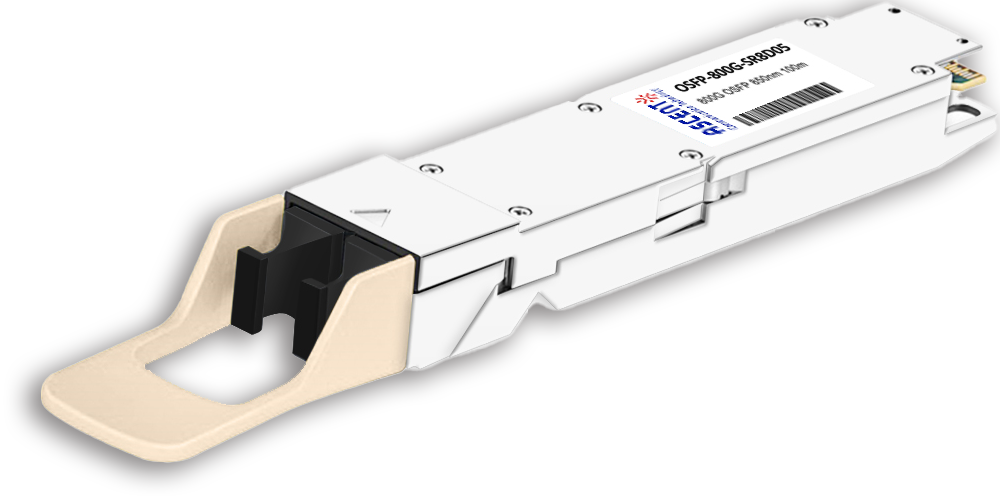
800G OSFP SR8 850 nm 100 m
OSFP-800G-SR8D-01 800 Gb/s OSFP SR8 850 nm 100 m Transceiver
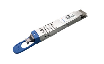
400G QSFP56-DD 10km
400G QSFP-DD 4X100G LR1 Optical Transceiver
400G QSFP-DD ZR+
QSFP-DD-ZR-80 400 Gb/s QSFP-DD 80 km Transceiver
400G QSFP-DD ER8 40 km
QSFP-DD-ER8-40 400 Gb/s QSFP-DD 40 km Transceiver
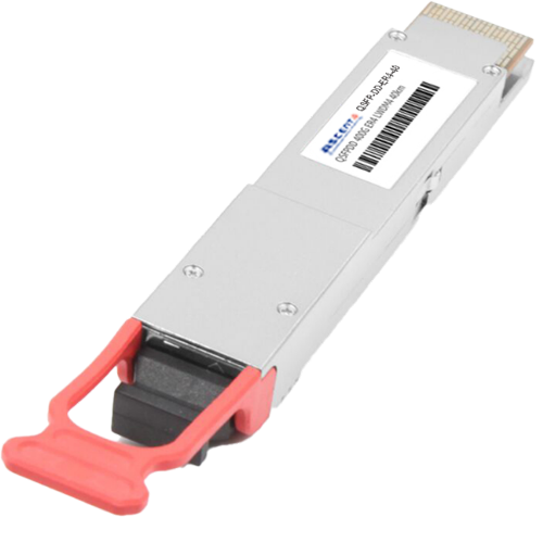
400G QSFP-DD 40 km
400 Gb/s QSFP-DD 40 km Transceiver
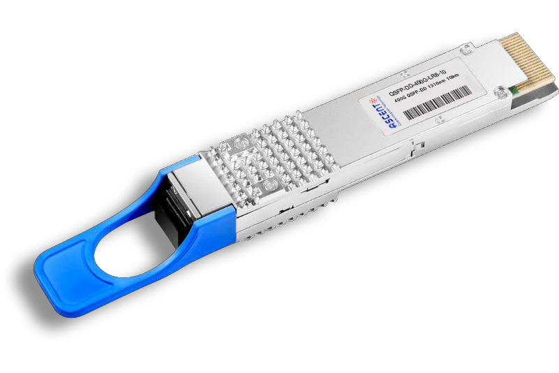
400G QSFP-DD LR8 1310 nm 10 km
QSFP-DD-LR8-10 400 Gb/s QSFP-DD LR8 10 km Transceiver

400G QSFP-DD LR4 CWDM 10 km
QSFP-DD-LR4-10 400 Gb/s QSFP-DD LR4 CWDM 10 km Transceiver
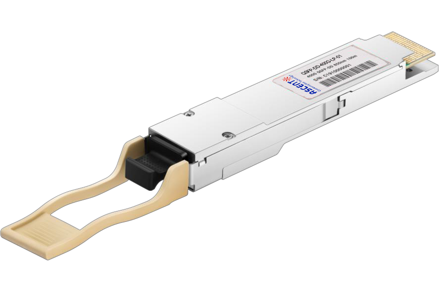
400G QSFP-DD SR8 850 nm 100 m
QSFP-DD-LP-01 400 Gb/s QSFP-DD SR8 100 m Transceiver
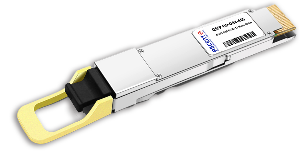
400G QSFP-DD DR4 500m
400 Gb/s QSFP-DD DR4 500m Transceiver
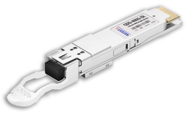
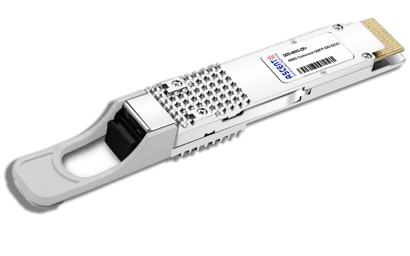
400G QSFP-DD DCO ZR
400G QSFP-DD DCO ZR Coherent Optical Transceiver
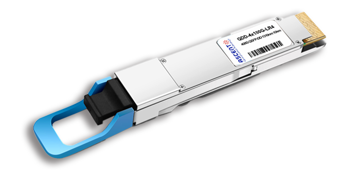
4X100G QSFP-DD LR4 10km
QDD 4x100G 1310nm LR 10 km Transceiver
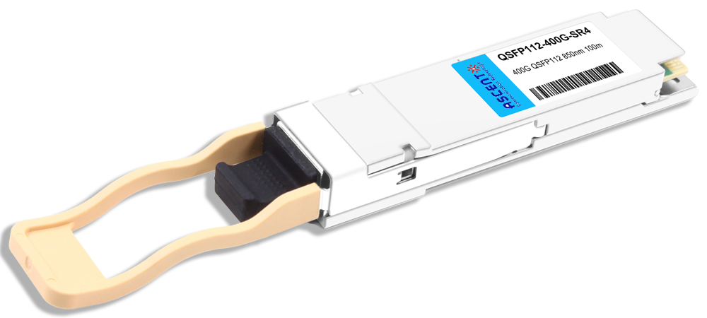
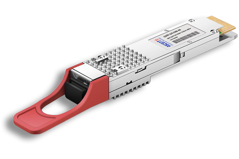
400G QSFP112 SR4 850 nm 100 m
QSFP112-400G-SR4-01 400 Gb/s QSFP112 SR4 850 nm 100 m Transceiver
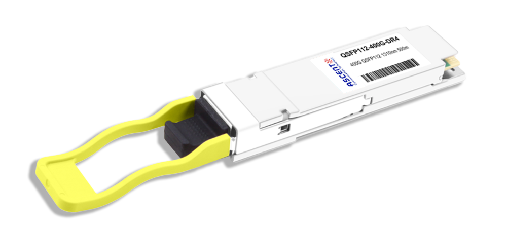
400G QSFP112 DR4 1310 nm 500 m
400G QSFP112 DR4 1310 nm Transceiver 500m
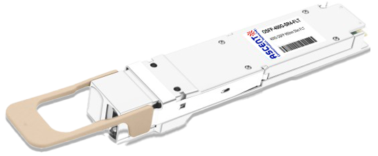
400G OSFP SR4 FLT 50m Transceiver
400 Gbps Multi-Mode 50m OSFP Transceiver
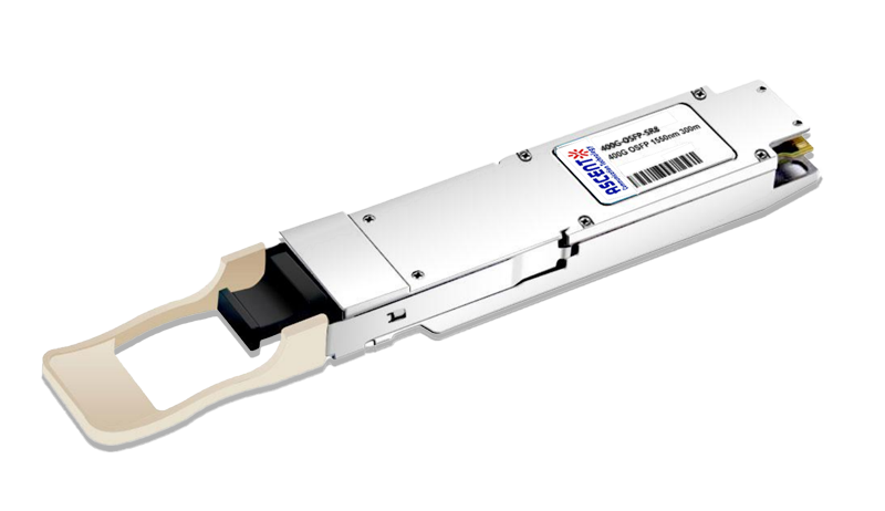
400G OSFP SR8 100m Transceiver
400 Gbps PSM8 Multi-Mode 100m OSFP Transceiver
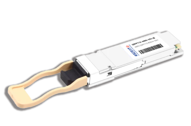
400G QSFP112 VR4 Transceiver
400G QSFP112 VR4
White Paper
Press Releases
Briefings 1
Briefings 2
Videos, etc.
QRG
Manual1
Manual2
Get in touch with our experts
Feedback