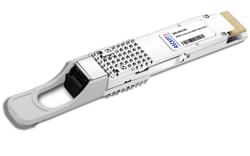
- FIBER OPTIC TRANSCEIVERS >800G & 400G Transceivers >400G QSFP-DD DCO ZR
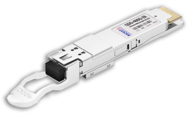
400G QSFP-DD DCO ZR
The ACT QDD-400G-ZR Series is a high-performance coherent optical transceiver designed for 400GbE data center interconnect (DCI), metro transport, and high-capacity backbone networks. Utilizing advanced coherent DSP technology and tunable C-band DWDM optics, the module enables transmission distances of up to 120 km without inline chromatic dispersion compensation, providing a compact and cost-effective solution for next-generation optical transport networks. The transceiver integrates a state-of-the-art 7 nm coherent DSP, ultra-narrow linewidth tunable lasers, high-speed modulators, and coherent receivers to deliver exceptional optical performance with 400G DP-16QAM modulation. Supporting both 400GbE and 4û100GbE client interfaces, the module offers flexible deployment across data center, carrier, and enterprise networks while reducing operational complexity and power consumption. Compliant with the QSFP-DD MSA and OIF 400ZR specifications, the QDD-400G-ZR supports comprehensive digital diagnostics, hot-pluggable operation, and seamless integration into modern switching and routing platforms. Its compact form factor, low power consumption, and Juniper-compatible option make it an ideal solution for DCI, metro, and cloud network applications.
ôñ QSFP-DD MSA compliant type 2B package
ôñ Up to 120km transmission distance
ôñ Client signal 400GbE or 4x100GbE
ôñ Line Modulation format 400G DP-16QAM
ôñ C-band tunable, supports 100/75GHz grid spacing, support 0.1GHz fine turning
ôñ TX power -13dBm to -9dBm tunable
ôñ Support ingress LF hold-off time configure
ôñ Support hitless firmware upgrade
ôñ Compact size (18.35 mm x 93.26 mm x 8.50 mm)
ôñ Duplex LC Receptacle
ôñ Operating case temperature: 0ô¯C to 75ô¯C
ôñ Maximum power consumption 18W (400GbE)
ôñ Single 3.3 V power supply
ôñ RoHS 2 compliant
Absolute Maximum Ratings
Parameter | Symbol | Min. | Typ. | Max. | Unit | Note | |
Storage Temperature | Ts | -40 | 85 | ô¯C | |||
Power Supply | Vcc | -0.3 | 3.3 | 3.6 | V | Not damaged | |
Relative Humidity | RH | 5 | 85 | % | Non-condensing | ||
Receiver Damage Threshold | PRdmg | 10 | dBm | Total optical power | |||
ESD Sensitivity | 1000 | V | |||||
Recommended Operating Conditions
Parameter | Symbol | Min. | Typ. | Max. | Unitd | Note | ||
Operating Case Temperature | Tc | 0 | 75 | ô¯C | ||||
Power Supply Voltage | Vcc | 3.135 | 3.3 | 3.465 | V | |||
Icc | 6.1 | A | 1 | |||||
Maximum Sustained Peak Current(<500ms) | 6.3 | A | ||||||
Maximum Instantaneous Peak Current(<50us) | 7.6 | A | ||||||
Electro-Static Discharge | ESD | 1000 | V | |||||
Power Consumption | PD | 18 | W | 1 | ||||
Relative Humidity | RH | 15 | 85 | % | ||||
Client Mode | 1 x 400GAUI-8 (OIF-400ZR-02.0) | |||||||
4 x 100GAUI-2 | ||||||||
Transmission Distance | 80 | 120 | Km | 30 to 40Km unamplified P2P link | ||||
Power Supply Noise | Vrip | 1% | DC-1MHz | |||||
2% | 1-10MHz | |||||||
Optical Electrical Characteristic
Tested under recommended operating conditions, unless otherwise noted
Parameters | Min. | Typ. | Max. | Unit | Note |
Format | ZR400-CFEC-16QAM | CFEC FEC, NCG 10.8dB SFF-8024 Media ID 3Eh/3Fh | |||
Baud Rate | 59.843750000ôÝ20ppm | ||||
Transmitter Frequency Range | 191.3
| 196.1
| THz
| OIF 400ZR app code 0x01/03 | |
193.7 | THz | OIF 400ZR app code 0x02, fixed wavelength | |||
Flexible DWDM Grid | 3.125 | GHz | OIF 400ZR app code 0x01/03 | ||
Frequency Fine Tuning Range | -5 | 5 | GHz | bright tuning, OIF 400ZRapp code 0x01/03 | |
Frequency Fine Tuning Step | 0.1 | GHz | OIF 400ZR app code 0x01/03 | ||
Laser Frequency Accuracy | -1.8 | 1.8 | GHz | ||
TX Spectral Upper Mask | (30.0, 0.0) (37.0,-10.0) (39.2,-15.0) (40.4,-20.0) | (GHz,dB) | Refer to OIF-400ZR-02.0 13.3.201a | ||
TX Spectral Lower Mask | (30.0,-9.0) (31.3,-20.0) (31.3,-35.0) | (GHz,dB) | Refer to OIF-400ZR-02.0 13.3.201b | ||
Transmitter Laser Disable Time | 100 | ms | |||
Transmitter Wavelength Wwitching Time | 60 | s | |||
Transmitter Laser Enable Time | 10 | s | |||
Tx Output Power(at Program Output Power Max) | -10 | -6 | dBm | At Programmed Output Power Max, transmit output power over wavelength, temperature, and aging. 0x01/03ã400ZR,DWDM amplified | |
-9 | -6 | dBm | 193.7THz, 0x02ã400ZR,Single wavelength, unamplified | ||
Transmit Output Power Adjustable Range | -13 | -9 | dBm | The absolute accuracy is ôÝ1dB OIF 400ZR app code 0x01/03 | |
Transmit Output Power Adjust Step | 0.1 | dB | OIF 400ZR app code 0x01/03 | ||
Optical Power Setting Accuracy | -1 | 1 | dB | Diff between setting and reporting | |
Output Power Monitor Accuracy | -1 | 1 | dB | ||
Power Stability | 0.5 | -0.5 | At fixed wavelength, room temp | ||
1 | -1 | At fixed wavelength, environment temp | |||
Total Output Power with Tx Disabled | -20 | ||||
Total Output Power During Wavelength Switching | -20 | ||||
Transmitter Reflectance | -20 | Looking into the Tx | |||
Inband (IB) OSNR | 40 | ||||
Out-of-Band (OOB) OSNR | 35 | ||||
Lorentzian Linewidth | 300 | Tx and LO | |||
Relative Intensity Noise | -140 | ||||
Mean I-Q Amplitude Imbalance | 1 | ||||
Transmitter Polarization Dependent Power | 1.5 | ||||
DC I-Q Offset (Mean per Polarization) | -26 | ||||
I-Q Instantaneous Offset | -20 | ||||
Receiver Operating Characteristic-Optical
Parameter | Min. | Typ. | Max. | Unit | Note |
Modulation Format | ZR400-CFEC-16QAM | CFEC FEC, Net Coding Gain(NCG) 10.8dB | |||
Baud Rate | 59.843750000ôÝ20ppm | ||||
Frequency Offset between Received Carrier and LO | -3.6 | +3.6 | GHz | ||
Input Power Range
| -12
| 0
| dBm
| Signal power of the channel for the 26dB OSNR tolerance 0x01ã400ZR,DWDM amplified | |
-20
| 0
| dBm
| 193.7THz,0x02ã 400ZR,Single wavelength, unamplified | ||
OSNR Tolerance | 26 | dB/0.1nm | Measured back-to-back with short optical channel | ||
RX Sensitivity | -20 | dBm | Inband (IB) OSNRãË34dB | ||
Non-Damaging Input Power | 10 | dBm | Total power | ||
Optical Input Power Monitor Accuracy | -2 | 2 | dB | ||
MAX Pre-FEC BER | 0.01 | 0.0125 | |||
Chromatic Dispersion Tolerance | 2400 | ps/nm | OSNR penalty < 0.5dB, when change in SOP is < 1 rad/ms. | ||
CD Monitor Accuracy | -200 | 200 | ps/nm | ||
Average PMD (DGD) Tolerance | 10(33) | ps | OSNR penalty<0.5dB | ||
DGD Monitor Accuracy | -15 | 15 | ps | 0~40ps | |
Peak PDL Tolerance | 3.5 | dB | Tolerance to peak PDL with < 1.8 dB penalty to OSNR tolerance (13.3.330) when change in SOP is < =1 rad/ms. Test configuration: PDL emulator applied before noise loading. | ||
Tolerance to Change in SOP | 50 | krad/s | With<0.5 dB OSNR penalty | ||
Optical Return Loss | 20 | dB | Optical reflectance at Rx connector input. | ||
Optical Rx_LOS Assert Threshold | -28 | -26 | -24 | dBm | OIF 400ZR app code 0x01, 0x02, 0x03 |
Optical Rx_LOS Hysteresis | 1 | 1.5 | 2.5 | dB | |
Optical Input Power Transient Tolerance | -2 | 2 | dB | Tolerance to change in input power with < 0.5 dB penalty to OSNR tolerance. The 20% to 80% rise/fall times for the input power change shall be no faster than 50 ôçs. | |
Service Recovery Time | 40 | ms | |||
Note: The transmitter and receiver comply with the 400GAUI-8 C2M and CEI-56G-VSR-PAM4 electrical specification, electrical interface definitions refer to IEEE Std 802.3-2018 Annex 120E. The data lines are AC-coupled and terminated in the module per the following figure from the QSFP-DD MSA.
Parameter | Symbol | Min | Max | Unit | Note |
400GAUI-8 C2M Electrical Characteristics | |||||
Transmitter(Module Output) | |||||
Signaling Rate, each Lane | 26.5625 ôÝ 100 ppm | GBd | PAM-4 | ||
AC Common-Mode Output Voltage (RMS) | RMS | 17.5 | mV | ||
Differential Voltage Pk-Pk | Vin, pp | 750 | 900 | mV | |
Near-End ESMW (Eye Symmetry Mask Width) | 0.265 | UI | |||
Near-End Eye Heightÿ¥Differential | 70 | mV | |||
Far-End ESMW | 0.2 | UI | |||
Far-End Eye Heightÿ¥Differential | 30 | mV | |||
Far-End Pre-Cursor ISI Ratio | -4.5 | 2.5 | % | ||
Differential Output Return Loss | Equation (83E-2) | IEEE Std 802.3-2018 Annex 120E | |||
Common to Differential Mode Conversion Return Loss | Equation (83E-3) | IEEE Std 802.3-2018 Annex 120E | |||
Differential Termination Mismatch | - | 10 | % | At 1 MHz | |
Transition Time(20% to 80%) | Trise/Tfall | 9.5 | Ps | 20% to 80% | |
DC Common Mode Voltage | Vcm | -350 | 2850 | mV | |
Receiver (Module Input) | |||||
Signaling Rate per Lane | 26.5625 ôÝ 100 ppm | GBd | PAM-4 | ||
Differential Pk-Pk Input Voltage Tolerance | Vout, pp | 900 | mV | ||
Differential Input Return Loss (Min) | Equation (83Eã5) | IEEE Std 802.3-2018 Annex 120E | |||
Differential to Common-Mode Input Return Loss (Min) | Equation (83Eã6) | IEEE Std 802.3-2018 Annex 120E | |||
Differential Termination Mismatch | 10 | % | |||
Module Stressed Input Test | See 120E.3.4.1 | IEEE Std 802.3-2018 Annex 120E | |||
Single-Ended Voltage Tolerance Range (Min) | -0.4 | 3.3 | V | ||
DC Common Mode Voltage(Min) | -350 | 2850 | mV | ||
Operating Characteristic-Electrical Low Speed
Parameter | Symbol | Min | Max | Unit | Note |
SCL and SDA | VOL | 0.4 | V | 0 | IOL(max)=3mA for fast mode, 20ma for Fast-mode plus |
VOH | Vcc+0.3 | V | Vcc-0.5 | ||
SCL and SDA | VIL | Vcc*0.3 | V | -0.3 | |
VIH | Vcc+0.5 | V | Vcc*0.7 | ||
Capacitance for SCL and SDA I/O Signal | Ci | 14 | pF | ||
Total Bus Capacitive Load for SCL and SDA
| Cb
| 100 | pF | For 400kHz clock rate, use 3.0 k Ohms Pull up resistor max. For 1000kHz clock rate, refer to Figure 45 (QSFP-DD-Hardware-rev5p0) | |
200
| pF
| For 400kHz clock rate, use 1.6 k Ohms pull up resistor max. For 1000kHz clock rate, refer to Figure 45 (QSFP-DD-Hardware-rev5p0) | |||
InitMode, ResetL and ModSelL IntL | VIL | 0.8 | V | -0.3 | |
VIH | VCC+0.3 | V | 2 | ||
|Iin| | 360 | uA | 0V<Vin<Vcc | ||
VOL | 0.4 | V | 0 | IOL=2.0mA | |
VOH | VCC+0.3 | V | VCC-0.5 | 10k ohms pull up to Host Vcc | |
ModPrsL | VOL | 0.4 | V | 0 | IOL=2.0mA |
VOH | ModPrsL can be implemented as a short-circuit to GND on the module |
Control and Status I/O Timing Characteristics
Parameter | Symbol | Min | Max | Unit | Note |
MgmtInit Duration | Max MgmtInit | 2000 | ms | 1 | |
ResetL Assert Time | t_reset_init | 10 | us | 2 | |
IntL Assert Time | ton_IntL | 200 | ms | 3 | |
IntL Deassert Time | toff_IntL | 500 | us | 4 | |
Rx LOS Assert Time | ton_los | 100 | ms | 5 | |
Rx LOS Assert Time (Optional Fast Mode) | ton_losf | 10 | ms | 6 | |
Rx LOS Deassert Time | toff_los | 100 | ms | ||
Tx Fault Assert Time | ton_Txfault | 200 | ms | 7 | |
Flag Assert Time | ton_flag | 200 | ms | 8 | |
Mask Assert Time | ton_mask | 100 | ms | 9 | |
Mask Deassert Time | toff_mask | 100 | ms | 10 | |
High Power Up State | 180 | s | |||
Software TX Disable Assert Time | 100 | ms | |||
Software TX Disable De-Assert Time | 10 | s |
Notes
1. Time from power on, hot plug or rising edge of reset until completion of the MgmtInit State.
2. Minimum pulse time on the ResetL signal to initiate a module reset.
3. Time from occurrence of condition triggering IntL until Vout:IntL=Vol.
4. Time from clear on read operation of associated flag until Vout:IntL=Voh. This includes deassert times for Rx
LOS,Tx Fault and other flag bits.
5. Time from Rx LOS condition present to Rx LOS bit set (value = 1b) and IntL asserted.
6. Time from Rx LOS state to Rx LOS bit set (value = 1b) and IntL asserted.
7. Time from Tx Fault state to Tx Fault bit set (value=1b) and IntL asserted.
8. Time from occurrence of condition triggering flag to associated flag bit set (value=1b) and IntL asserted.
9. Time from mask bit set (value=1b) until associated IntL assertion is inhibited.
10. Time from mask bit cleared (value=0b) until associated IntL operation resumes.
IIC 2-Wire Characterisitcs
Parameter | Symbol | Fast Mode (400 KHz) | Fast Mode Plus(1 MHz) | Unit | Conditions | ||
Min | Max | Min | Max | ||||
Clock Frequency | fSCL | 0 | 400 | 0 | 1000 | KHz | |
Clock Pulse Width Low | tLOW | 1.3 | 0.5 | ôçs | |||
Clock Pulse Width High | tHIGH | 0.6 | 0.26 | ôçs | |||
Time Bus Free before New Transmission Can Start | tBUF | 20 | 1 | ôçs | Between STOP and START and between ACK and ReStart | ||
START Hold Time | tHD.STA | 0.6 | 0.26 | ôçs | The delay required between SDA becoming low and SCL starting to go low in a START | ||
START Setup Time | tSU.STA | 0.6 | 0.26 | ôçs | The delay required between SCL becoming high and SDA starting to go low in a START | ||
Data In Hold Time | tHD.DAT | 0 | 0 | ôçs | |||
Data In Setup Time | tSU.DAT | 0.1 | 0.1 | ôçs | |||
Input Rise Time | tR | 300 | 120 | ns | From (VIL,MAX=0.3*Vcc) to (VIH, MIN=0.7*Vcc) | ||
Input Fall Time | tF | 300 | 120 | ns | From (VIH,MIN=0.7*Vcc) to (VIL,MAX=0.3*Vcc) | ||
STOP Setup Time | tSU.STO | 0.6 | 0.6 | us | |||
STOP Hold Time | tHD.STO | 0.6 | 0.26 | us | |||
Aborted Sequence-Bus Release | Deselect_Abort | 2 | 2 | ms | Delay from a host de-asserting ModSelL (at any point in a bus sequence) to the QSFP-DD module releasing SCL and SDA | ||
ModSelL Setup Time1 | tSU.ModSelL | 2 | 2 | ms | ModSelL Setup Time is the setup time on the select lines before the start of a host initiated serial bus sequence | ||
ModSelL Hold Time1 | tHD.ModSelL | 2 | 2 | ms | ModSelL Hold Time is the delay from completion of a serial bus sequence to changes of module Select status | ||
Serial Interface Clock Holdoff ãClock Stretchingã | T_clock_hold | 500 | 500 | us | Maximum time the QSFP-DD module may hold the SCL line low before continuing with a read or write operation | ||
Complete Single Sequential Write | tWR | 40 | 40 | ms | Complete (up to) 4 Byte Write | ||
Endurance (Write Cycles) | 50K | 50K | cycles | Module Case Temperature = 75ô¯C | |||
Note: When the host has determined that module is QSFP-DD, the management registers can be read to determine alternate supported ModSelL set up and hold times.


800G OSFP DAC Cable
800G IB NDR OSFP to 4xOSFP RHS Hairtail+ Direct Attach Copper Cable
800G OSFP ACC Cable
800G OSFP Breakout to 4x200G OSFP Active Copper Cable
800G OSFP DR8 1310 nm 500 m
800 Gb/s DR8 OSFP 500m Optical Transceiver
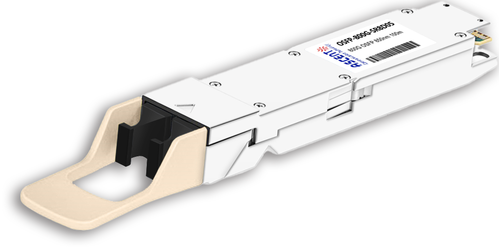
800G OSFP SR8 850 nm 100 m
OSFP-800G-SR8D-01 800 Gb/s OSFP SR8 850 nm 100 m Transceiver
400G QSFP56-DD 10km
400G QSFP-DD 4X100G LR1 Optical Transceiver
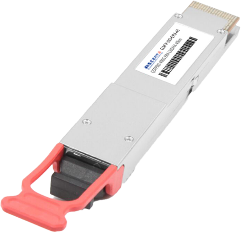
400G QSFP-DD ZR+
QSFP-DD-ZR-80 400 Gb/s QSFP-DD 80 km Transceiver
400G QSFP-DD ER8 40 km
QSFP-DD-ER8-40 400 Gb/s QSFP-DD 40 km Transceiver
400G QSFP-DD 40 km
400 Gb/s QSFP-DD 40 km Transceiver
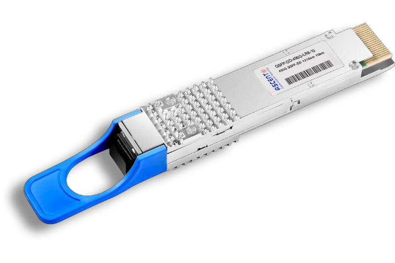
400G QSFP-DD LR8 1310 nm 10 km
QSFP-DD-LR8-10 400 Gb/s QSFP-DD LR8 10 km Transceiver

400G QSFP-DD LR4 CWDM 10 km
QSFP-DD-LR4-10 400 Gb/s QSFP-DD LR4 CWDM 10 km Transceiver
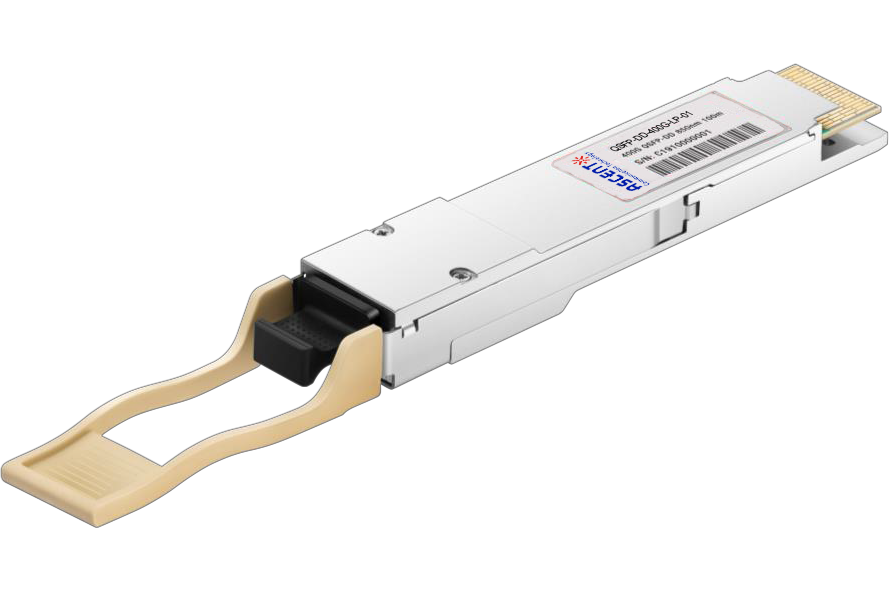
400G QSFP-DD SR8 850 nm 100 m
QSFP-DD-LP-01 400 Gb/s QSFP-DD SR8 100 m Transceiver
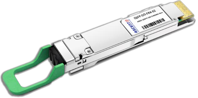
400G QSFP-DD FR4 2km
400 Gb/s QSFP-DD FR4 2 km DDM Transceiver
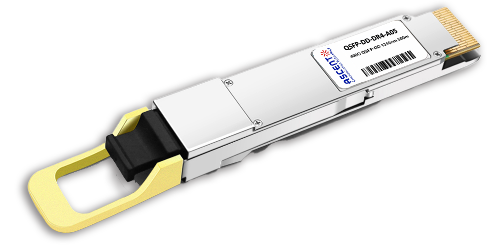
400G QSFP-DD DR4 500m
400 Gb/s QSFP-DD DR4 500m Transceiver
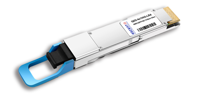
4X100G QSFP-DD LR4 10km
QDD 4x100G 1310nm LR 10 km Transceiver
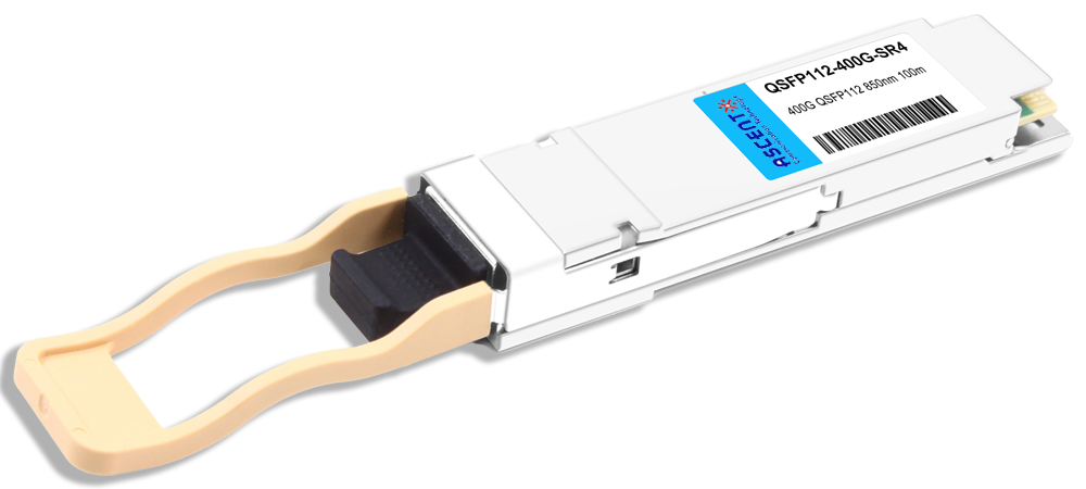
400G QSFP112 SR4 850 nm 100 m
QSFP112-400G-SR4-01 400 Gb/s QSFP112 SR4 850 nm 100 m Transceiver
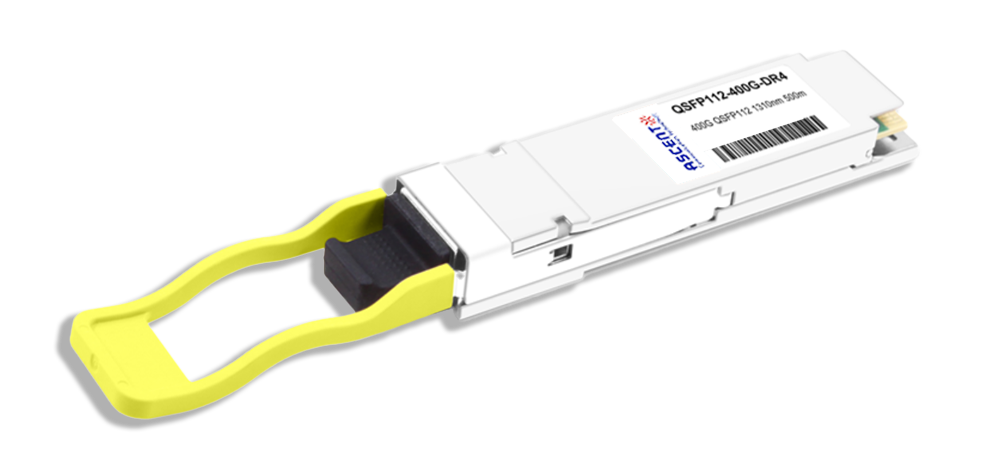
400G QSFP112 DR4 1310 nm 500 m
400G QSFP112 DR4 1310 nm Transceiver 500m
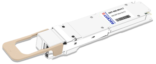
400G OSFP SR4 FLT 50m Transceiver
400 Gbps Multi-Mode 50m OSFP Transceiver
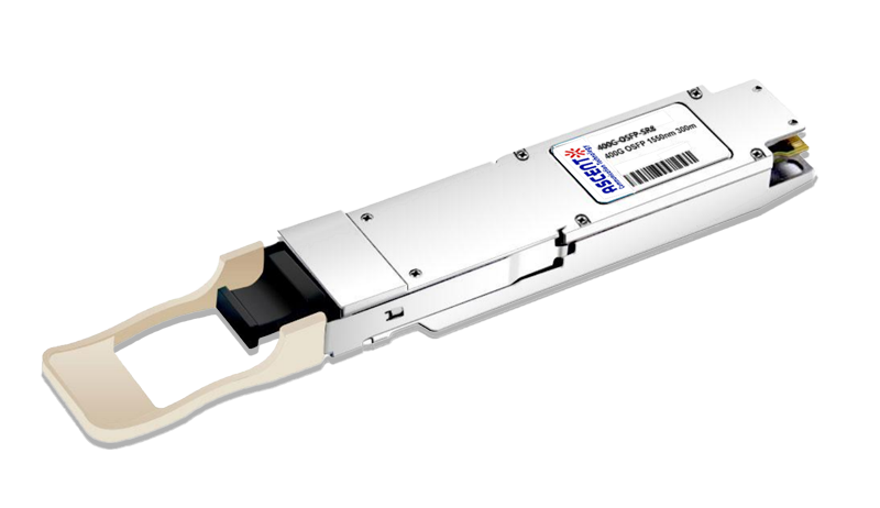
400G OSFP SR8 100m Transceiver
400 Gbps PSM8 Multi-Mode 100m OSFP Transceiver
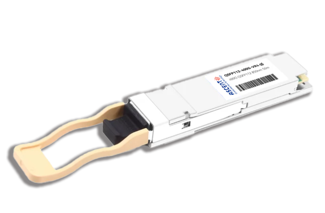
400G QSFP112 VR4 Transceiver
400G QSFP112 VR4
White Paper
Press Releases
Briefings 1
Briefings 2
Videos, etc.
QRG
Manual1
Manual2
Get in touch with our experts
Feedback