- FIBER OPTIC TRANSCEIVERS >PON Transceivers >GPON OLT SFP 2.5G Class C+ 20 km
GPON OLT SFP 2.5G Class C+ 20 km
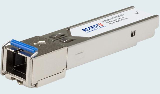
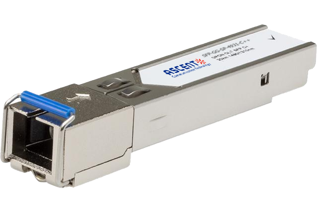
ASCENTãs GPON OLT transceiver SFP-GG-SP-4931 C+ is designed for optical line terminal (OLT) for ITU-T G.984.2 Class C+ requirements Network transmission. The optical transceiver is compliant with the Small Form- Factor Pluggable (SFP) Multi- Source Agreement (MSA). The GPON OLT SFP module is contained in a SFP package with SC/UPC receptacle connector. The module consists 1490 nm DFB laser, InGaAs APD, Preamplifier and WDM filter in a high-integrated optical sub-assembly, and it transmit up to 2.5 Gbps of continuous data at 1490 nm, and receives 1.25 Gbps burst-mode data at 1310 nm. The module data link up to 20 km in 9/125 ôçm single-mode fiber. Ascent GPON SFP is a low cost point to multi point (P2MP) Fiber to the Home, Business or Curb (FTTX) GPON OLT transceiver. It is fabricated with a rugged die cast metal housing and cage assembly. Commercial and industrial temperature ranges are available. It is IEC 60825-1 Class I laser safety compliant and meets the EEC Directive 2002/95/EC for RoHS compliance.
ã Single-fiber bi-directional data links asymmetric TX 2488 Mbps / RX 1244 Mbps application
ã Single fiber bi-directional data links asymmetric TX 2488Mbps/RX1244Mbps application
ã 1490nm continuous-mode DFB laser transmitter and 1310nm burst-mode APD-TIA receiver
ã Small Form Factor Pluggable package with SC/UPC Connector
ã Single 3.3V power supply
ã DDMI function available with internally calibrated mode
ã Digital burst RSSI function to monitor the input optical power level
ã LVPECL compatible data input/output interface
ã LVTTL transmitter disable control
ã LVTTL transmitter laser fault alarm
ã Fast LVTTL receiver Signal Detect (SD) indication response
ã Low EMI and excellent ESD protection
ã International Class1 laser safety certified
ã Operating temperature range:
Commercial: -5ô¯C to 70ô¯C
ã Complies with EU Directive 2015/863/EU
ã Complies with SFP Multi-Source Agreement (MSA) SFF-8074i
ã Complies with ITU-T G.984.2 Amendment 1
ã Complies with FCC 47 CFR Part 15, Class B
ã Complies with FDA 21 CFR 1040.10 and 1040.11 except for deviations pursuant to Laser Notice No.
50, dated June 24, 2007
ã Complies with SFF-8472
ã Compatible with TR-NWT-000870 4.1 ESD sensitivity classification Class2
ã Compatible with Telcordia GR-468-CORE
Absolute Maximum Ratings
Parameter | Symbol | Min. | Typ. | Max. | Unit | Notes |
Storage Ambient Temperature | TSTG | -40 | 85 | ô¯C | ||
Storage Humidity | HS | 0 | 90 | ô¯C | ||
Operating Humidity | Ho | 5 | 85 | % | ||
Power Supply Voltage | VCC | 0 | 3.6 | V | ||
Receiver Damaged Threshold | +4 | dBm |
Parameter | Symbol | Min. | Typ. | Max. | Unit | Notes |
Operating Case Temperature | TC | -5 | 70 | ô¯C | ||
Power Supply Voltage | VCC | 3.13 | 3.3 | 3.47 | V | |
Power Consumption | PW | 1.65 | W | |||
Data Rate | TX 2.488 / RX 1.244 | Gbps |
Parameter | Symbol | Min. | Typ. | Max. | Unit | Notes |
Total Supply Current | ICC | 500 | mA | |||
Transmitter | ||||||
Transmitter Differential Input Voltage | 400 | 2400 | mV | |||
Tx_Fault Output Voltage - High | VOH | 2.4 | Vcc | V | LVTTL | |
Tx_Fault Output Voltage - Low | VOL | 0 | 0.4 | V | LVTTL | |
Tx_Disable Input Voltage - High | VIH | 2 | Vcc | V | LVTTL | |
Tx_Disable Input Voltage - Low | VIL | 0 | 0.8 | V | LVTTL | |
Input Differential Impedance | ZIN | 85 | 100 | 115 | öˋ | |
Receiver | ||||||
Receiver Differential Output Voltage | 600 | 1600 | mV | LVPECL, DC Coupled | ||
SD Output Voltage - High | VOH | 2.4 | Vcc | V | LVTTL | |
SD Output Voltage - Low | VOL | 0 | 0.4 | V | LVTTL | |
Reset Input Voltage - High | VIH | 2.0 | Vcc | V | LVTTL | |
Reset Input Voltage - Low | VIL | 0 | 0.8 | V | LVTTL | |
RSSI Trigger Input Voltage - High | VIH | 2.0 | Vcc | V | LVTTL | |
RSSI Trigger Input Voltage - Low | VIL | 0 | 0.8 | V | LVTTL | |
Output Differential Impedance | ZOUT | 90 | 100 | 110 | öˋ | |
Parameter | Symbol | Min. | Typ. | Max. | Unit | Notes |
Transmitter | ||||||
Average Output Power | POUT | +3 | +7 | dBm | ||
Center Wavelength | ö£C | 1480 | 1500 | nm | ||
Spectral Width (-20dB) | ãö£ | 1 | nm | |||
Side Mode Suppression Ratio | SMSR | 30 | ||||
Extinction Ratio | ER | 8.2 | dB | PRBS 223-1+72CID @2.488Gbit/s | ||
Transmitter and Dispersion Penalty | TDP | 1 | dB | Transmit on 20km SMF | ||
Transmitter OFF Power | POFF | -39 | dBm | |||
Output Eye Diagram | Compliant with ITU-T G.984.2 | |||||
Transmitter Reflectance | -10 | dB | ||||
Receiver | ||||||
Center Wavelength | ö£C | 1260 | 1360 | nm | ||
Receiver Sensitivity | SEN | -30 | dBm | 1 | ||
Input Saturation Power (Overload) | SAT | -12 | dBm | |||
Dynamic Range | 15 | dB | Figure of Burst Mode Receiver Dynamic Range in GPON System | |||
Receiver Reflectance | -15 | dB | ||||
1. PRBS 223-1+72CID @1244Mbps, transmitter is operating, BER ãÊ1û10-10.
Burst Mode Receiver Dynamic Range in GPON System

Burst Receiver Timing Sequence


Receiver Timing Characteristics
Parameter | Symbol | Min. | Typ. | Max. | Unit | Notes |
Guard Time | TG | 32 | bit | |||
Reset Pulse Width | TR | 16 | bit | 1 | ||
Receiver Amplitude Recovery Time | TSETTLE | 24 | bit | 2 | ||
TSETTLE_E | 16 | bit | ||||
Signal Detect Assert Time | TA | 25 | ns | |||
Signal Detect De-Assert Time | TD | 10 | ns |
1. Reset pulse support 2 modes in Burst Receiver Timing Sequence figure.
2. SD signal pulls down immediately after Reset signal, and pulls up while detected RX burst signal till the next Reset signal.

RSSI Characteristics
Parameter | Symbol | Min. | Typ. | Max. | Unit | Notes |
RSSI Trigger-Low | 0 | 0.8 | V | |||
RSSI Trigger-High | 2.0 | Vcc | V | |||
RSSI Trigger Delay | TD | 0 | 3000 | ns | ||
Optical Signal During Time | TONT | 300 | ns | |||
RSSI Trigger Width | TW | 300 | TONT - TD | ns | ||
I2C Access Prohibited Time | Tp | 500 | ö¥s |


White Paper
Press Releases
Briefings 1
Briefings 2
Videos, etc.
QRG
Manual1
Manual2
Get in touch with our experts
Feedback