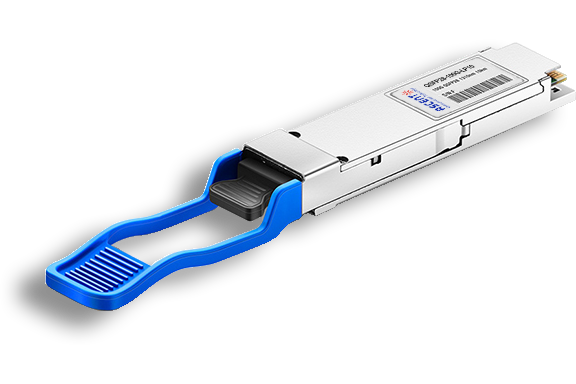
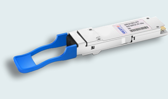
- FIBER OPTIC TRANSCEIVERS >200G & 100G Transceivers >100G QSFP28 FR Single ö£ 1310 nm 2 km

100G QSFP28 FR Single ö£ 1310 nm 2 km
Ascentãs QSFP28 FR 100Gb/s transceiver is a compact, high-performance single-lambda optical module designed for 2 km transmission over single-mode fiber. Compliant with IEEE 100GBASE-FR, it delivers a reliable 100G Ethernet link in a QSFP28 form factor, making it ideal for high-density data center and enterprise network deployments. Leveraging PAM4 modulation and integrated DSP technology, the module converts four high-speed electrical lanes into a single 1310 nm optical wavelength, enabling efficient, cost-optimized short-reach connectivity. A cooled EML laser on the transmit side and a PIN photodiode receiver ensure stable signal performance and excellent link margin, while RS-FEC support enhances transmission robustness. Designed for operational efficiency, the product offers low power consumption (<3.5 W) and supports standard digital diagnostic monitoring (DDM) for real-time performance visibility. With its proven reliability and compact footprint, it is well suited for switch-to-switch, router interconnect, and 100G data center networking applications.
ôñ IEEE 100GBASE-FR compliant
ôñ 100GE Single Protocol (103.125Gb/s)
ôñ CAUI-4 compliant ã 4 x 25.78Gb/s
ôñ 100GAUI-4 compliant ã 4 x 26.562Gb/s
ôñ RS-FEC (544,514) FEC coder/decoder function
ôñ Power Consumption < 3.5 W Max
ôñ Operating case temperature: 0 ô¯C to +70 ô¯C
ôñ Single cooled 100Gb/s 1310nm EML
ôñ Single PIN PD + low-power TIA
ôñ SFF-8636 management interface
Absolute Maximum Ratings
Parameter | Symbol | Min. | Max. | Unit | Note |
Power Supply Voltage | Vcc | 0 | +3.6 | V | +3.3 V |
Storage Temperature | -40 | 85 | ô¯C | ||
Optical Receiver Input | - | +5.5 | dBm | Average |
Operating Environment
Parameter | Symbol | Min. | Typ. | Max. | Unit | Note |
Power Supply Voltage | Vcc | 3.135 | 3.3 | 3.465 | V | |
Supply Voltage Noise Tolerance | PSNR | - | - | 66 | mV | 10 Hz to 10 MHz |
Maximum Power Consumption | - | - | 3.5 | W | Target | |
Power Supply Current | -- | - | 1010.1 | mA | Steady state | |
Operating Case Temperature | TC | 0 | 25 | 70 | ô¯C |
Optical Characteristics
Parameter | Min. | Typ. | Max. | Unit | Note |
Transmitter | |||||
PAM4 Signaling Rate | 53.125 ôÝ 100 ppm | GBd | |||
Lane Wavelengths | 1304.5 to 1317.5 | nm | |||
Side-Mode Suppression Ratio (SMSR) | 30 | dB | |||
Average Launch Power | -3.1 | 4 | dBm | 1 | |
Outer Optical Modulation Amplitude (OMAouter) for TDECQ<1.4 dB | -0.1 | 4.2 | dBm | ||
Outer Optical Modulation Amplitude (OMAouter) for 1.4 dB ãÊTDECQ ãÊ3.4 dB | -1.5 + TDECQ | dBm | |||
Transmitter and Dispersion Penalty Eye Closure for PAM4 (TDECQ) | 3.4 | dB | |||
|TDECQ ã TECQ| | 2.5 | dB | |||
Over/Under-Shoot | 22 | % | |||
Transmitter Power Excursion | 2 | dBm | |||
Average Launch Power of OFF Transmitter | -15 | dBm | |||
Extinction Ratio | 3.5 | dB | |||
Optical Return Loss Tolerance | 17.1 | dB | |||
Transmitter Reflectance | -26 | dB | 2 | ||
Transmitter Transition Time | 17 | ps | |||
RIN15.5 OMA | -136 | dB/Hz | |||
Receiver | |||||
PAM4 Signaling Rate | 53.125 ôÝ 100 ppm | GBd | |||
Lane Wavelengths | 1304.5 to 1317.5 | nm | |||
Damage Threshold | 5 | dBm | 3 | ||
Average Receive Power | -7.1 | 4 | dBm | 4 | |
Receive Power (OMAouter) | 4.2 | dBm | |||
Receiver Reflectance | -26 | dB | |||
Receiver Sensitivity (OMAouter) | -4.5, TECQ -5.9 | dBm | |||
Stressed Receiver Sensitivity (OMAouter) | -2.5 | dBm | 5 | ||
| Conditions of Stressed Receiver Sensitivity Test | 6 | ||||
Stressed Eye Closure for PAM4 (SECQ) | 3.4 | dB | |||
SECQ ã 10*Log10(Ceq) | - | dB | 7 | ||
Notes:
1. Average launch power, each lane (min) is informative and not the principal indicator of signal strength. A transmitter with launch power below this value cannot be compliant; however, a value above this does not ensure compliance.
2. Transmitter reflectance is defined looking into the transmitter.
3. The receiver shall be able to tolerate, without damage, continuous exposure to an optical signal having this average power level.
4. Average receive power, each lane (min) is informative and not the principal indicator of signal strength. A received power below this value cannot be compliant; however, a value above this does not ensure compliance.
5. Measured with conformance test signal at TP3 (see 100G Lambda MSA 100G-FR - ãTechnical Specification, Rev. 2.0 clause 3.11) for the BER specified in IEEE Std 802.3cd clause 140.1.1.
6. These test conditions are for measuring stressed receiver sensitivity. They are not characteristics of the receiver.
7. Ceq is a coefficient defined in IEEE Std 802.3-2018 clause 121.8.5.3 which accounts for reference equalizer noise enhancement.
OMA Outer

Receiver Sensitivity

RX_LOS Characteristics
Parameter | Symbol | Min. | Typ. | Max. | Unit | Notes |
Receiver Loss of Signal Indicator Assert Level | RX_LOS | -30 | - | -7.5 | dBm | Average power |
Receiver Loss of Signal Indicator De-assert Level | RX_LOS | - | - | -7 | dBm | Average power |
Electrical Characteristics
Parameter | Min. | Typ. | Max. | Unit | Notes |
Transmitter (Each Lane) | |||||
Differential Pk-Pk Input Voltage Tolerance | 900 | - | - | mV | at TP1a |
Differential Termination Mismatch | - | - | 10 | % | at TP1 |
Single-Ended Input Voltage Tolerance Range | -0.4 to -3.3 | - | V | at TP1a | |
DC Common Mode Voltage | -350 | - | 2850 | mV | at TP1 |
Receiver (Each Lane, at TP4) | |||||
AC Common-Mode Output Voltage (RMS) | - | - | 17.5 | mV | |
Differential Output Voltage | - | - | 900 | mV | |
Eye Width | 0.57 | - | - | UI | |
Eye Height, Differential | 228 | - | - | mV | |
Vertical Eye Closure | - | - | 5.5 | dB | |
Differential Termination Mismatch | - | - | 10 | % | |
Transition Time (20% to 80%) | 12 | - | - | ps | |
DC Common Mode Boltage | -350 | - | 2850 | mV | |
Note: Electrical Rx output is squelched for loss of optical input signal.
Reference Test Points


200G QSFP DD LR4 10km
200 Gb/s QSFP DD LR4 10 km Transceiver
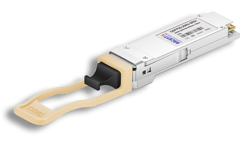
200G QSFP56 SR4 850 nm 100 m
QSFP56-200G-SR01 200 Gb/s QSFP56 SR4 850 nm 100 m Transceiver

100G QSFP28 LX4 2km
100 Gb/s 2km QSFP28 LX4 Transceiver

100G QSFP28OA LR4 10km
100 Gb/s 10 km QSFP28 LR4 Transceiver

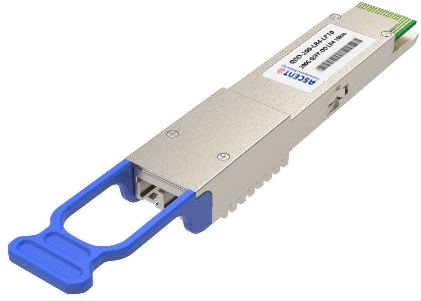
100G QSFP28 ZR4 1310 nm 80 km
QSFP28-100G-LP80 QSFP28 100 Gbps ZR4 Transceiver
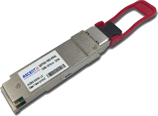
100G QSFP28 ER4L 1310 nm 40 km
QSFP28-100G-LP40 100 Gb/s 40 km QSFP28 ER4 Lite Transceiver

100G QSFP28 ER4 1310 nm 40 km
100 Gb/s 40 km QSFP28 ER4 Transceiver
100G QSFP28 LR4 1310 nm 10 km
QSFP28-100G-LP10 100 Gb/s 10km QSFP28 LR4 Transceiver
100G QSFP28 LR Single ö£ 10 km
100G QSFP28 LR1 10 km Single Channel

100G QSFP28 DR Single ö£ 500 m
QSFP28 100G DR Single Lambda Transceiver
100G QSFP28 CWDM4 1310 nm 2 km
QSFP28-100G-LP02 QSFP28 100 Gbps CWDM4 Transceiver
100G QSFP28 PSM4 1310 nm 2 km
QSFP28-100G-PSM4 100 Gb/s 1310 nm 2 km Transceiver
100G QSFP28 SR4 850 nm 100 m
QSFP28-100G-SR01 100 Gb/s SR4 850 nm 100 m Transceiver

100G QSFP28 SR01 BIDI MMF 850nm 100m
QSFP28 BIDI 100 Gb/s SR Transceiver 100m

100G QSFP28 BIDI 80km
QSFP28 BIDI 100 Gb/s ZR4 Transceiver 80km

100G QSFP28 BIDI 40km
QSFP28 BIDI 100 Gb/s ER Transceiver 40km

100G QSFP28 EZR4 100km
QSFP28 100Gb/s EZR4 Transceiver 100km

100G SFP56 ER1 30km
SFP56-DD 100G-ER1 Optical Transceiver 30km

100G SFP56 LR1 10km
SFP56-DD 100G-LR1 Optical Transceiver 10km
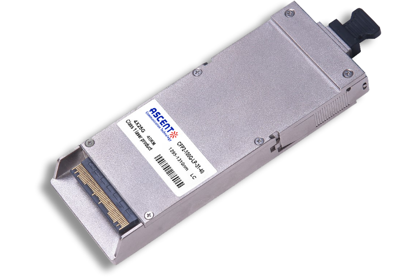
100G CFP2 ER4 40 km
CFP2-LP-31-40 100 Gb/s CFP2 ER4 40 km Transceiver
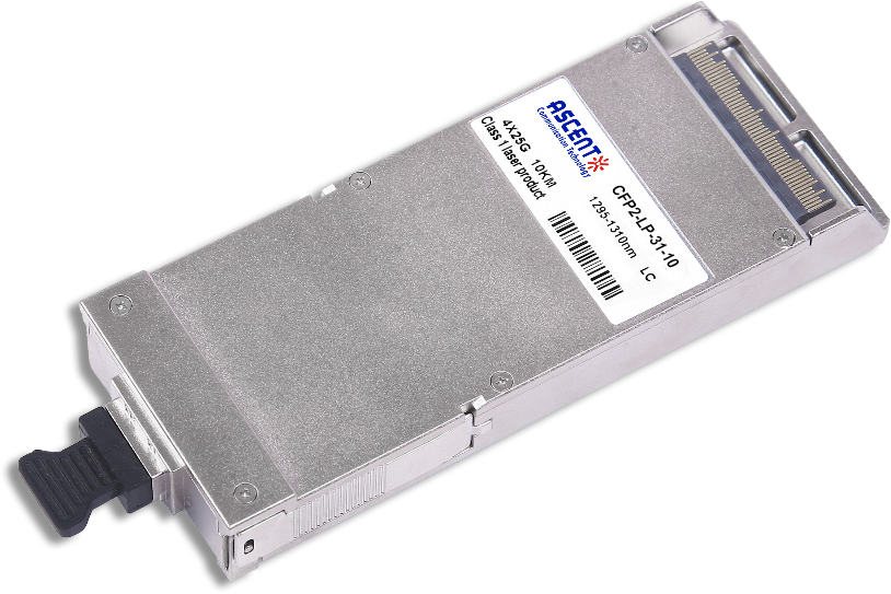
100G CFP2 LR4 10 km
CFP2-LP-31-10 100 Gb/s CFP2 LR4 10 km Transceiver
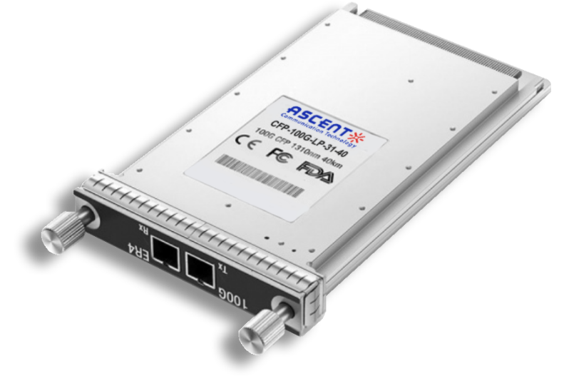
100G CFP ER4 40 km
CFP-LP-31-40 100 Gb/s CFP ER4 40 km Transceiver
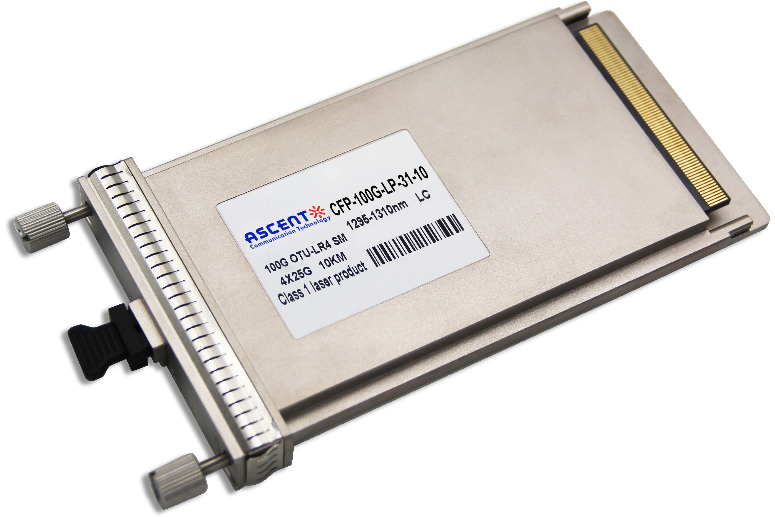
100G CFP LR4 10 km
CFP-LP-31-10 100 Gb/s CFP LR4 10 km Transceiver
White Paper
Press Releases
Briefings 1
Briefings 2
Videos, etc.
Manual1
Manual2
Get in touch with our experts
Feedback