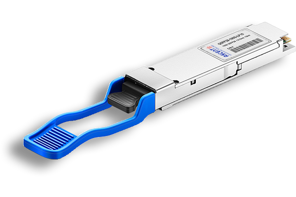
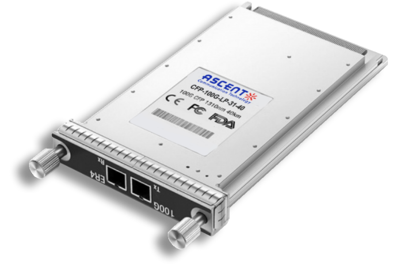
- FIBER OPTIC TRANSCEIVERS >200G & 100G Transceivers >100G CFP2 ER4 40 km
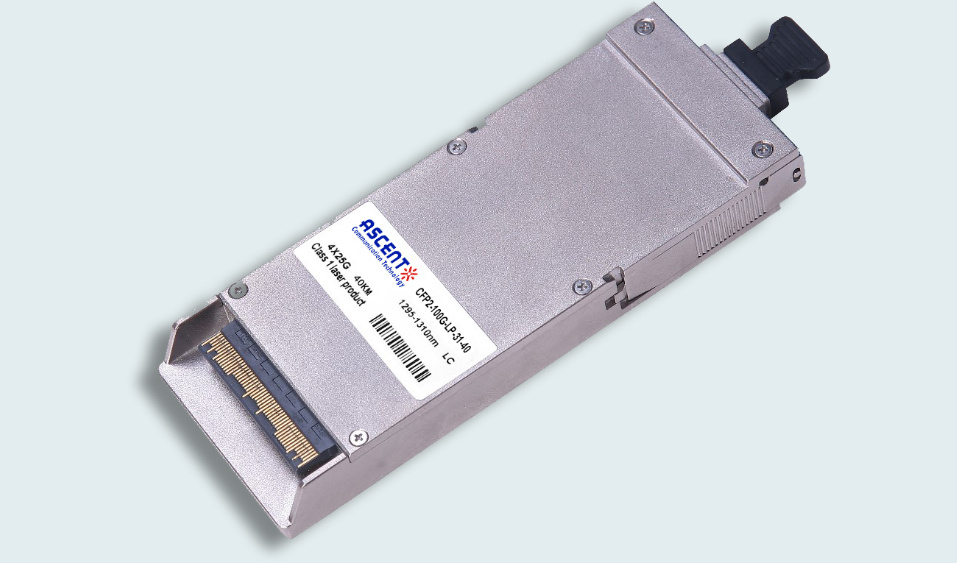
100G CFP2 ER4 40 km
Ascentãs 100G CFP2 LR4 optical Transceiver integrates receiver and transmitter path on one module. In the transmit side, four lanes of serial data streams are recovered, retimed, and passed to four laser drivers. The laser drivers control four EMLs (Electric-absorption Modulated Lasers) with center wavelength of 1296 nm, 1300nm, 1305nm and 1309 nm. The optical signals are multiplexed to a single-mode fiber through an industry standard LC connector. In the receive side, the four lanes of optical data streams are optically de-multiplexed by the integrated optical de-multiplexer. Each data stream is recovered by a SOA to amplify, then go to PIN photo-detector and trans-impedance amplifier, retimed. This module features a hot-pluggable electrical interface, low power consumption and MDIO management interface.
ã Compliant with 100GBASE-ER4
ã Support line rates from 103.125 Gbps to 111.81 Gbps
ã Integrated LAN WDM EML TOSA, SOA, ROSA for up to 40 km reach over SMF
ã Digital Diagnostics Monitoring Interface
ã Duplex LC optical receptacle
ã No external reference clock
ã Single 3.3 V power supply
ã Case operating temperature range:0 ô¯C to 70 ô¯C
ã Power dissipation < 9W
Absolute Maximum Ratings
Parameter | Symbol | Min. | Typ. | Max. | Unit | Notes |
Storage Temperature | Ts | ã40 | ã | 85 | ô¯C | |
Relative Humidity | RH | 5 | ã | 95 | % | |
Power Supply Voltage | VCC | ã0.3 | ã | 4 | V | |
Signal Input Voltage | Vccã0.3 | ã | Vcc+0.3 | V | ||
Receive Input Optical Power (Damage Threshold) | Pdmg | 5.0 | dBm |
Low Speed Electrical Characteristics
Parameter | Symbol | Min.. | Typ. | Max. | Unit | Notes |
Supply Currents and Voltages | ||||||
Voltage | Vcc | 3.2 | 3.3 | 3.4 | V | With Respect to GND |
Supply Current | Icc | 2.3 | A | |||
Power Dissipation | Pwr | 9.0 | W | |||
Power Dissipation (Low Power Mode) | Plp | 2.5 | W | |||
Low Speed Control and Sense Signals, 3.3 V LVCMOS | ||||||
Outputs Low Voltage | VOL | 0.2 | V | IOH=100 ö¥A | ||
Output High Voltage | VOH | Vccã0.2 | V | IOH=ã100 ö¥A | ||
Input Low Voltage | VIL | ã0.3 | 0.8 | V | ||
Input High Voltage | VIH | 2 | Vcc3+0.3 | V | ||
Input Leakage Current | IIN | ã10 | 10 | ö¥A | ||
Low Speed Control and Sense Signals, 1.2 V LVCMOS | ||||||
Outputs Low Voltage | VOL | ã0.3 | 0.2 | V | ||
Output High Voltage | VOH | 1.0 | 1.5 | V | ||
Output Low Current | IOL | 4 | mA | |||
Output High Current | IOH | ã4 | mA | |||
Input Low Voltage | VIL | ã0.3 | 0.36 | V | ||
Input High Voltage | VIH | 0.84 | 1.5 | V | ||
Input Leakage Current | IIN | ã100 | 100 | ö¥A | ||
Input Capacitance | C | 10 | pF | |||
MDC Clock Rate | 0.1 | 4 | MHz | |||
High Speed Electrical Specifications
Parameter | Symbol | Min. | Max. | Unit | Notes |
Transmitter Electrical Input from Host | |||||
Differential Voltage pkãpk | 100 | 1200 | mV | ||
Common Mode Noise (rms) | 17.5 | mV | |||
Differential Termination Mismatch | 10 | % | |||
Transition Time | 10 | ps | 20/80 % | ||
Common Mode Voltage | ã0.3 | 2.8 | V | ||
Eye Width | EW15 | 0.46 | UI | At10ã15probability | |
Eye Height | EH15 | 100 | mV | At 10ã15 probability | |
Receiver Electrical Output to Host | |||||
Differential Voltage pkãpk | 100 | 1200 | mV | ||
Common Mode Noise (rms) | 17.5 | mV | |||
Differential Termination Mismatch | 10 | % | |||
Transition Time | 9.5 | ps | 20/80 % | ||
Vertical Eye Closure | VEC | 6.5 | dB | ||
Eye Width | EW15 | 0.57 | UI | At 10ã15 probability | |
Eye Height | EH15 | 240 | mV | At 10ã15 probability | |
Optical Characteristics
Parameter | Symbol | Min. | Typ. | Max. | Unit | Notes |
Transmitter | ||||||
Signaling Speed per Lane | 25.78125 | Gbps | ||||
Wavelength Assignment | ö£0 | 1294.53 | 1295.56 | 1296.59 | nm | |
ö£1 | 1299.02 | 1300.05 | 1301.09 | nm | ||
ö£2 | 1303.54 | 1304.58 | 1305.63 | nm | ||
ö£3 | 1308.09 | 1309.14 | 1310.19 | nm | ||
Rate Tolerance | ã100 | 100 | ppm | 1 | ||
SideãMode Suppression Ratio | SMSR | 30 | dB | |||
Total Launch Power | 8.9 | dBm | ||||
Average Launch Power, per Lane | Pavg | ã2.9 | 2.9 | dBm | ||
Extinction Ratio | ER | 8 | dB | |||
Optical Modulation Amplitude, per Lane (OMA) | OMA | 0.1 | dBm | |||
Difference in Launch Power between any Two Lanes (Average and OMA) | 3.6 | dB | ||||
Transmitter and Dispersion Penalty, per Lane | TDP | 2.5 | dB | |||
Average Launch Power of OFF Transmitter, per Lane | ã30 | dBm | ||||
Transmitter Reflectance | ã12 | dB | ||||
Output Eye Mask definition {X1, X2, X3, Y1, Y2, Y3} | {0.25, 0.4, 0.45, 0.25, 0.28, 0.4} | |||||
Receiver | ||||||
Signaling Rate, Each Lane | 25.78125 | Gbps | ||||
Rate Tolerance | ã100 | 100 | ppm | 1 | ||
Average Receive Power, per Lane | Pavg | ã20.9 | 4.5 | dBm | ||
Receive Power, per Lane (OMA) | 4.5 | dBm | ||||
Difference in Launch Power between any Two Lanes (Average and OMA) | 4.5 | dB | ||||
Receiver Sensitivity (OMA), per Lane | Rsen | ã21.4 | dBm | 2 | ||
Stressed Receiver Sensitivity (OMA), per Lane | SRS | ã17.9 | dBm | |||
Stressed Receiver Sensitivity Test Conditions | ||||||
Vertical Eye Closure Penalty, per Lane | VECP | 3.5 | dB | |||
Stressed Sys J2 Jitter, per Lane | J2 | 0.3 | UI | 3 | ||
Stressed Sys J9 Jitter, per Lane | J9 | 0.47 | UI | 3 | ||
Receiver Reflectance | ã26 | dB | ||||
Los Assert | Plos_on | ã36 | dBm | |||
Los DeãAssert | Plos_off | ã24 | dBm | |||
Los Hysteresis | 0.5 | 4 | dB | |||
Notes:
1. From nominal rate
2. Receiver sensitivity (OMA), per lane, is informative.
3. Vertical eye closure penalty, stressed eye J2 Jitter, and stressed eye J9 Jitter are test conditions for measuring stressed receiver sensitivity. They are not characteristics of the receiver.

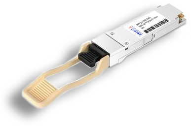
200G QSFP DD LR4 10km
200 Gb/s QSFP DD LR4 10 km Transceiver
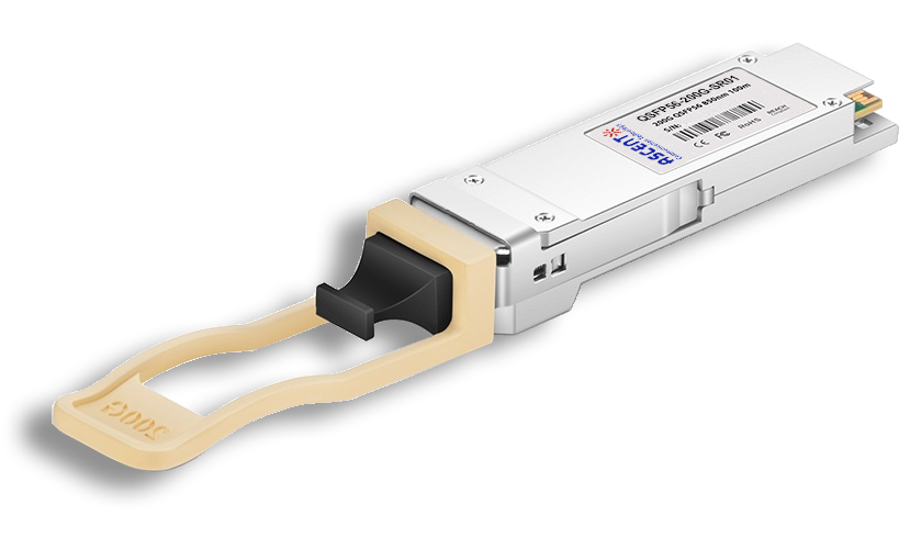
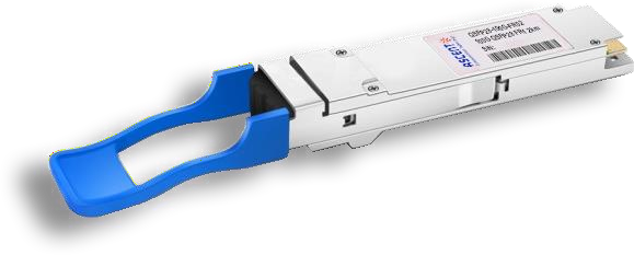
200G QSFP56 SR4 850 nm 100 m
QSFP56-200G-SR01 200 Gb/s QSFP56 SR4 850 nm 100 m Transceiver

100G QSFP28 LX4 2km
100 Gb/s 2km QSFP28 LX4 Transceiver

100G QSFP28OA LR4 10km
100 Gb/s 10 km QSFP28 LR4 Transceiver

100G QSFP28 ZR4 1310 nm 80 km
QSFP28-100G-LP80 QSFP28 100 Gbps ZR4 Transceiver
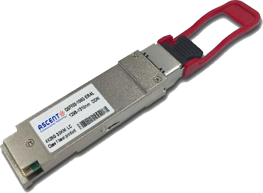
100G QSFP28 ER4L 1310 nm 40 km
QSFP28-100G-LP40 100 Gb/s 40 km QSFP28 ER4 Lite Transceiver

100G QSFP28 ER4 1310 nm 40 km
100 Gb/s 40 km QSFP28 ER4 Transceiver
100G QSFP28 LR4 1310 nm 10 km
QSFP28-100G-LP10 100 Gb/s 10km QSFP28 LR4 Transceiver
100G QSFP28 LR Single ö£ 10 km
100G QSFP28 LR1 10 km Single Channel

100G QSFP28 DR Single ö£ 500 m
QSFP28 100G DR Single Lambda Transceiver
100G QSFP28 CWDM4 1310 nm 2 km
QSFP28-100G-LP02 QSFP28 100 Gbps CWDM4 Transceiver
100G QSFP28 PSM4 1310 nm 2 km
QSFP28-100G-PSM4 100 Gb/s 1310 nm 2 km Transceiver
100G QSFP28 SR4 850 nm 100 m
QSFP28-100G-SR01 100 Gb/s SR4 850 nm 100 m Transceiver
100G QSFP28 FR Single ö£ 1310 nm 2 km
100G QSFP28 FR 2km Transceiver

100G QSFP28 SR01 BIDI MMF 850nm 100m
QSFP28 BIDI 100 Gb/s SR Transceiver 100m

100G QSFP28 BIDI 80km
QSFP28 BIDI 100 Gb/s ZR4 Transceiver 80km

100G QSFP28 BIDI 40km
QSFP28 BIDI 100 Gb/s ER Transceiver 40km

100G QSFP28 EZR4 100km
QSFP28 100Gb/s EZR4 Transceiver 100km

100G SFP56 ER1 30km
SFP56-DD 100G-ER1 Optical Transceiver 30km

100G SFP56 LR1 10km
SFP56-DD 100G-LR1 Optical Transceiver 10km
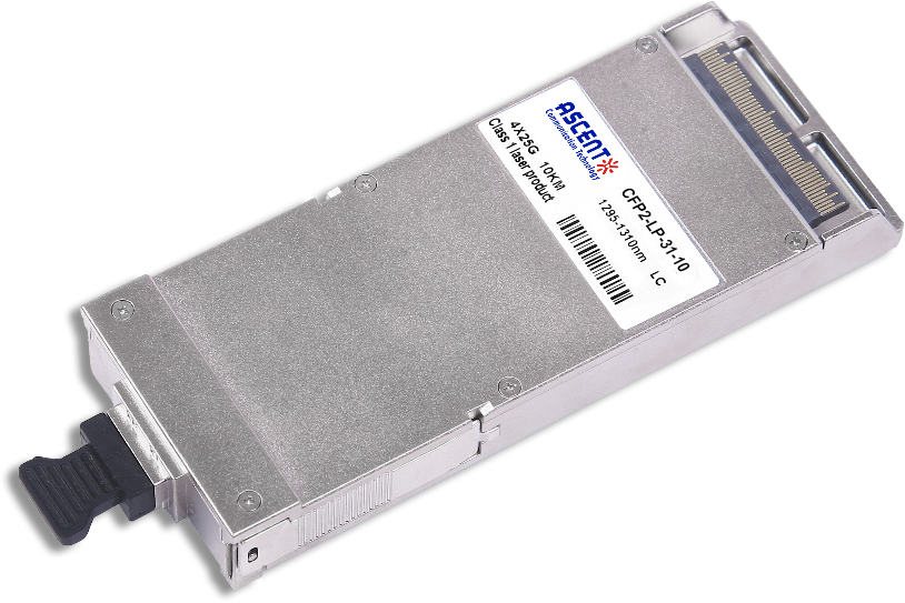
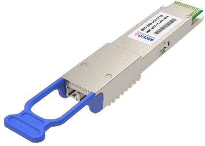
100G CFP2 LR4 10 km
CFP2-LP-31-10 100 Gb/s CFP2 LR4 10 km Transceiver
100G CFP ER4 40 km
CFP-LP-31-40 100 Gb/s CFP ER4 40 km Transceiver
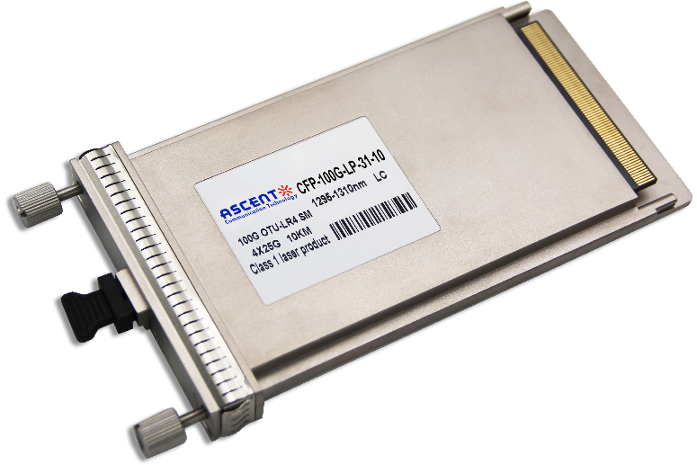
100G CFP LR4 10 km
CFP-LP-31-10 100 Gb/s CFP LR4 10 km Transceiver
White Paper
Press Releases
Briefings 1
Briefings 2
Videos, etc.
QRG
Manual1
Manual2
Get in touch with our experts
Feedback