- FIBER OPTIC TRANSCEIVERS >200G & 100G Transceivers >100G SFP56 LR1 10km

100G SFP56 LR1 10km
Ascentãs 100G LR1 SFP56-DD optical transceiver, SFP56-DD-LR10 is designed for using in 100-Gigabit Ethernet links up to 10km over Single-Mode Fiber (SMF). It is compliant with the SFP56-DD MSA, IEEE802.3CU, 100G Lambda 100G LR1 and CAUI-4 (no FEC). Digital diagnostics functions are available via the I2C interface, as specified by the SFP56-DD MSA. The module incorporates 1 channel optical signal, on 1311nm center wavelength, operating at 100Gbps data rate. This module can convert 2 channels of 53Gbps (PAM4) electrical input data to 1 channel of 106Gbps (PAM4) optical signal, and also can convert 1 channel of 106Gbps (PAM4) optical signal to 2 channels of 53Gbps (PAM) electrical output data. The optical interface uses a Duplex LC connector. The high performance cooled EML transmitter and high sensitivity PIN receiver provide superior performance for 100Gigabit Ethernet applications up to 10km links.
ôñ Compliant to 100G Lambda MSA 100G LR1-10
ôñ Full-duplex transceiver module
ôñ 1x106.25Gb/s(PAM4) optical interface
ôñ 2x53.125Gb/s(PAM4) electrical interface
ôñ 106.25Gbps PAM4 based on a cooled EML TOSA transmitter
ôñ 106.25Gbps PAM4 PIN Receiver
ôñ 3.5W maximum power consumption
ôñ Hot-pluggable SFP56-DD form factor
ôñ Maximum link length of 10km on G.652 SMF with KP-FEC
ôñ Duplex LC receptacles
ôñ Built-in digital diagnostic functions
ôñ Operating case temperature range: 0 to 70ô¯C
ôñ Single 3.3V power supply
ôñ RoHS compliant (lead free)
Absolute Maximum Ratings
Parameter | Symbol | Min. | Max. | Unit |
Supply Voltage | Vcc | -0.3 | 3.6 | V |
Input Voltage | Vin | -0.3 | Vcc+0.3 | V |
Storage Temperature | Ts | -20 | 85 | ô¯C |
Case Operating Temperature | Tc | 0 | 70 | ô¯C |
Humidity (non-condensing) | Rh | 5 | 85 | % |
Recommended Operating Conditions
Parameter | Symbol | Min. | Typ. | Max | Unit |
Supply Voltage | Vcc | 3.13 | 3.3 | 3.47 | V |
Operating Case Temperature | Tc | 0 | - | 70 | ô¯C |
Data Rate Per Lane | fd | - | 106.25 | - | Gb/s |
Humidity | Rh | 5 | - | 85 | % |
Power Consumption | Pm | - | 3 | 3.5 | W |
Link Distance with G.652 | D | - | - | 10 | km |
Electrical Characteristics
Parameter | Symbol | Min. | Typ. | Max | Unit | Note |
Differential Input Impedance | Zin | 90 | 100 | 110 | ohm | |
Differential Output Impedance | Zout | 90 | 100 | 110 | ohm | |
Differential Input Voltage Amplitude | öVin | - | - | 1600 | mVp-p | 1 |
Differential Output Voltage Amplitude | öVout | - | - | 900 | mVp-p | 2 |
Notes:
1. Differential input voltage amplitude is measured between TxnP and TxnN.
2. Differential output voltage amplitude is measured between RxnP and RxnN.
Optical Characteristics
Parameter | Symbol | Min. | Typ. | Max. | Unit | Notes |
Transmitter | ||||||
Centre Wavelength | ö£c | 1304.5 | - | 1317.5 | nm | - |
Side-Mode Suppression Ratio | SMSR | 30 | - | - | dB | - |
Average Launch Power | Pout | -1.4 | - | 4.5 | dBm | - |
Transmitter and Dispersion Eye Closure(TDECQ) | TDECQ | - | - | 3.4 | dB | |
Extinction Ratio | ER | 3.5 | - | - | dB | - |
Average Launch Power of OFF transmitter | - | - | -30 | dB | - | |
Receiver | ||||||
Centre Wavelength | ö£c | 1304.5 | - | 1317.5 | nm | - |
Receiver Sensitivity in OMAouter | RXsen | - | - | -6.1 | dBm | 1 |
Average Receive Power | Pin | -7.7 | - | 4.5 | dBm | - |
Receiver Reflectance | - | - | -26 | dB | - | |
LOS Assert | - | -13 | - | dBm | - | |
LOS De-Assert ã OMA | - | -11 | - | dBm | - | |
LOS Hysteresis | 0.5 | - | - | dB | - | |
1. Measured with conformance test signal at TP3 for BER = 2.4E-4 Pre-FECs.
Diagnostic Monitoring Interface (Optional)
The following digital diagnostic characteristics are defined over the normal operating conditions unless otherwise specified.
Parameter | Symbol | Min. | Max. | Unit | Notes |
Temperature Monitor Absolute Error | DMI_Temp | -3 | +3 | ô¯C | Over operating temperature range |
Supply Voltage Monitor Absolute Error | DMI _VCC | -0.1 | 0.1 | V | Over full operating range |
Channel RX Power Monitor Absolute Error | DMI_RX_Ch | -2 | 2 | dB | 1 |
Channel Bias Current Monitor | DMI_Ibias_Ch | -10% | 10% | mA | |
Channel TX Power Monitor Absolute Error | DMI_TX_Ch | -2 | 2 | dB | 1 |
1. Due to measurement accuracy of different single mode fibers, there could be an additional +/-1 dB fluctuation, or a +/- 3 dB total accuracy.
2. Digital diagnostics functions are available via the I2C interface as specified by SFP-DD MIS. The SFP-DD MIS management memory is shown in below figure.

The Lower Memory Overview

Page 00h Memory Overview

Page 01h Memory Overview
3. Due to eight-bit addresses, This limits the management memory that can be directly accessed by the host to 256 bytes, which is divided in Lower Memory (addresses 00h through 7Fh) and Upper Memory (addresses 80h through FFh).
4. The addressing structure of the additional internal management memory1 is shown in below figure.
The management memory inside the module is arranged as a unique and always host accessible address space of 128 bytes (Lower Memory) and as multiple upper address subspaces of 128 bytes each (Pages),
only one of which is selected as host visible in Upper Memory. A second level of Page selection is possible for Pages for which several instances exist (e.g. where a bank of pages with the same Page number exists).

Page 13h Memory Overview

Page 14h Memory Overview

5. This structure supports a flat 256 byte memory for passive copper modules and permits timely access to addresses in the Lower Memory, e.g. Flags and Monitors. Less time critical entries, e.g. serial ID information and threshold settings, are available with the Page
Select function in the Lower Page. For more complex modules which require a larger amount of management memory the host needs to use dynamic mapping of the various Pages into the host addressable Upper Memory address space, whenever needed.
6. The management memory map has been designed largely after the CMIS memory map where pages and banks are used in order to enable time critical interactions between host and module while expanding the memory size. This memory map has been changed in
order to accommodate just two electrical lanes and to limit the required memory. The single address approach is used as found in QSFP.
Regulatory Compliance
Ascentãs SFP56-DD-LR10 transceivers are Class 1 Laser Products. They meet the requirements of the following standards.
Feature | Standard |
Laser Safety | EC 60825-1:2014 (3rd Edition) EN 60825-2:2004+A1+A2 |
Electrical Safety | EN 62368-1: 2014 IEC 62368-1:2014 UL 62368-1:2014 |
Environmental Protection | Directive 2011/65/EU with amendment(EU)2015/863 |

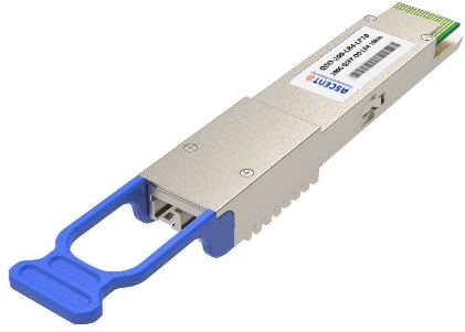
200G QSFP DD LR4 10km
200 Gb/s QSFP DD LR4 10 km Transceiver
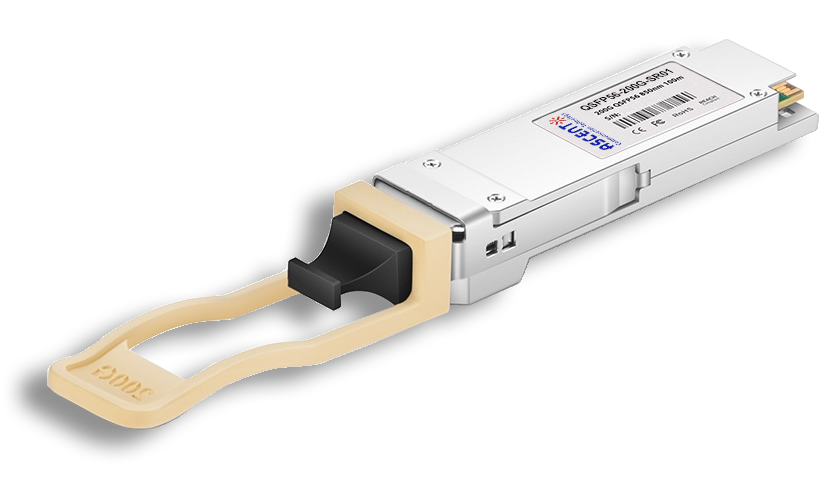
200G QSFP56 SR4 850 nm 100 m
QSFP56-200G-SR01 200 Gb/s QSFP56 SR4 850 nm 100 m Transceiver

100G QSFP28 LX4 2km
100 Gb/s 2km QSFP28 LX4 Transceiver

100G QSFP28OA LR4 10km
100 Gb/s 10 km QSFP28 LR4 Transceiver

100G QSFP28 ZR4 1310 nm 80 km
QSFP28-100G-LP80 QSFP28 100 Gbps ZR4 Transceiver
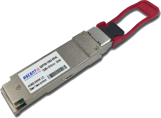
100G QSFP28 ER4L 1310 nm 40 km
QSFP28-100G-LP40 100 Gb/s 40 km QSFP28 ER4 Lite Transceiver

100G QSFP28 ER4 1310 nm 40 km
100 Gb/s 40 km QSFP28 ER4 Transceiver
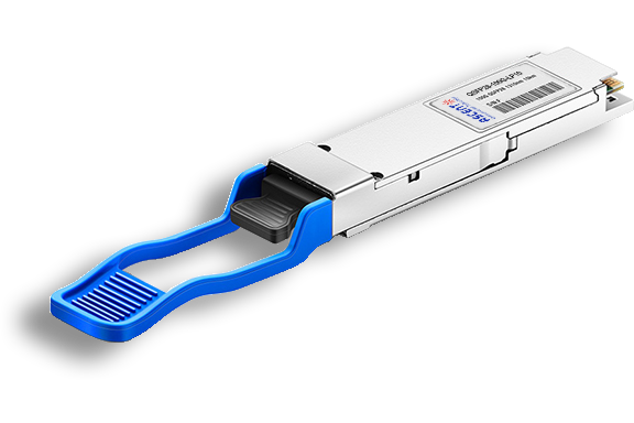
100G QSFP28 LR4 1310 nm 10 km
QSFP28-100G-LP10 100 Gb/s 10km QSFP28 LR4 Transceiver
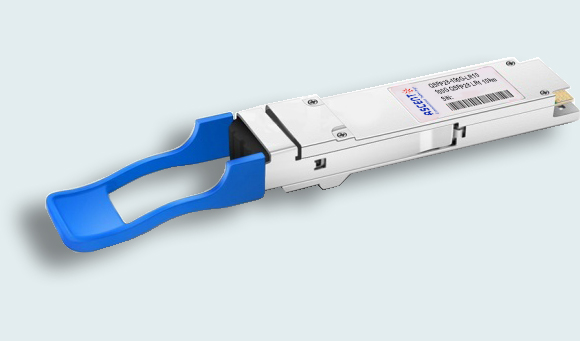
100G QSFP28 LR Single ö£ 10 km
100G QSFP28 LR1 10 km Single Channel

100G QSFP28 DR Single ö£ 500 m
QSFP28 100G DR Single Lambda Transceiver
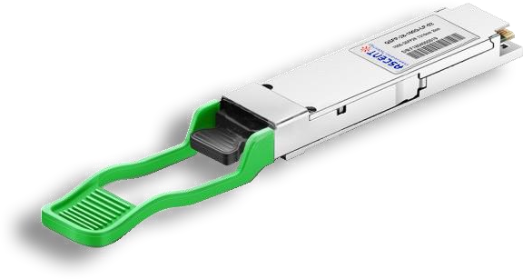
100G QSFP28 CWDM4 1310 nm 2 km
QSFP28-100G-LP02 QSFP28 100 Gbps CWDM4 Transceiver
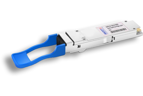
100G QSFP28 PSM4 1310 nm 2 km
QSFP28-100G-PSM4 100 Gb/s 1310 nm 2 km Transceiver
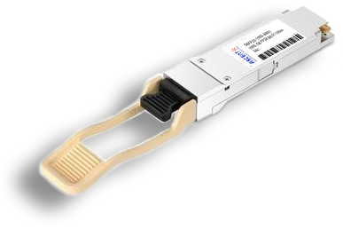
100G QSFP28 SR4 850 nm 100 m
QSFP28-100G-SR01 100 Gb/s SR4 850 nm 100 m Transceiver
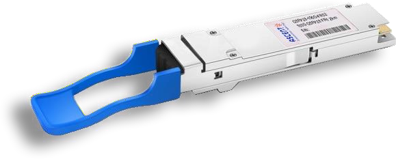
100G QSFP28 FR Single ö£ 1310 nm 2 km
100G QSFP28 FR 2km Transceiver

100G QSFP28 SR01 BIDI MMF 850nm 100m
QSFP28 BIDI 100 Gb/s SR Transceiver 100m

100G QSFP28 BIDI 80km
QSFP28 BIDI 100 Gb/s ZR4 Transceiver 80km

100G QSFP28 BIDI 40km
QSFP28 BIDI 100 Gb/s ER Transceiver 40km

100G QSFP28 EZR4 100km
QSFP28 100Gb/s EZR4 Transceiver 100km

100G SFP56 ER1 30km
SFP56-DD 100G-ER1 Optical Transceiver 30km
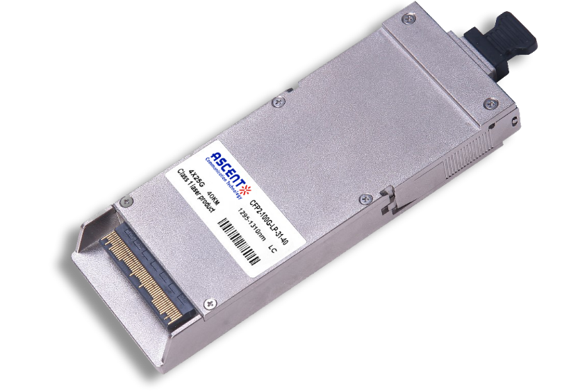
100G CFP2 ER4 40 km
CFP2-LP-31-40 100 Gb/s CFP2 ER4 40 km Transceiver
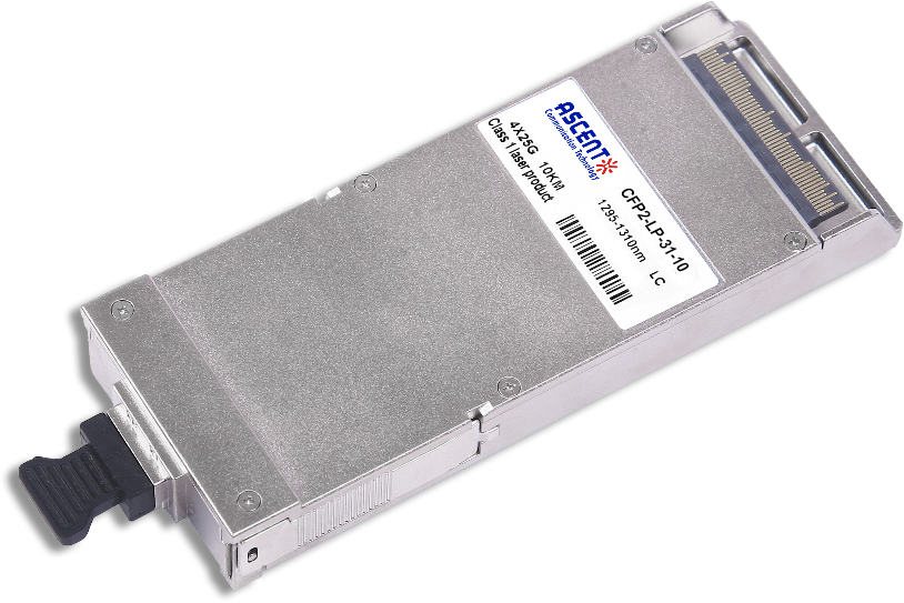
100G CFP2 LR4 10 km
CFP2-LP-31-10 100 Gb/s CFP2 LR4 10 km Transceiver
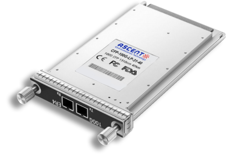
100G CFP ER4 40 km
CFP-LP-31-40 100 Gb/s CFP ER4 40 km Transceiver
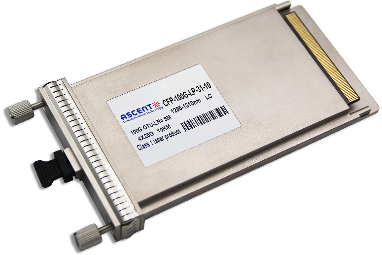
100G CFP LR4 10 km
CFP-LP-31-10 100 Gb/s CFP LR4 10 km Transceiver
White Paper
Press Releases
Briefings 1
Briefings 2
Videos, etc.
QRG
Manual1
Manual2
Get in touch with our experts
Feedback