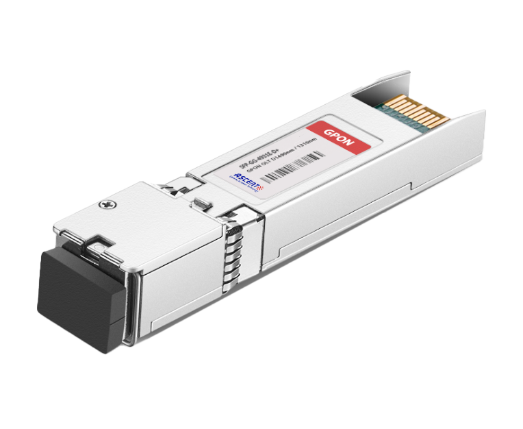
- FIBER OPTIC TRANSCEIVERS >PON Transceivers >XGSPON N2 SFP Transceiver

XGSPON N2 SFP Transceiver
The XGSPON N2 & GPON C+ Combo SFP+ is a dual-mode optical transceiver that supports both next-gen XGSPON and legacy GPON in a single compact SFP+ module. Designed for smooth network evolution, it enables operators to serve GPON and XGSPON users simultaneouslyãwithout hardware changes. Fully compliant with ITU-T G.984.5 (2014)/Amd.2 (10/2020) standards, this hot-pluggable module delivers high reliability, low power consumption, and excellent optical sensitivity. It integrates easily into major OLT platforms, supporting flexible deployments across a wide range of environments. With the XGSPON N2 & GPON C+ Combo SFP+, service providers can cut upgrade costs, extend infrastructure lifespan, and accelerate rollout of ultra-fast broadbandãall with one simple solution. The transceiver is a combination of XGS-PON OLT and GPON OLT optical transceiver in an SFP+ housing. It is designed to support both the XGS-PON OLT and the GPON OLT specifications over a single fiber via coarse wave division multiplexing. The XGS-PON bidirectional link is configured with 1270nm/1577nm optics and the GPON link is configured with 1310nm/1490nm optics. The 1270nm and 1310nm optical burst mode receivers incorporate APD/TIA optics for maximum sensitivity. The 10G transmitter incorporates a 1577nm EML laser assembly and the 2.5G transmitter incorporates a 1490nm DFB laser assembly. The transmitters can be controlled by the LVTTL Tx_DISABLE function and the receivers incorporates the LVTTL Rx_SD output. The transceiver is designed to support up to 32/64 subscribers over distances of up to 20km.
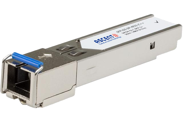
ôñ SFP+ Package
ôñ 3.3V DC power supply
ôñ 4 Lambda
ôñ SC receptacle optical connector
ôñ Hot pluggable
ôñ 2x10 SFP+ Electrical Interface
ôñ ITU-T G.984.2 Class C+ compliant
ôñ ITU-T G.987.2 Class C+ compliant
ôñ ITU-T G.9807.1 Class C+ compliant
ôñ 1577nm CW Mode EML
o 9.95328Gb/s data rate
o LVCML AC Coupled input
ôñ 1490nm CW Mode DFB Laser
o 2.48832Gb/s data rate
o LVPECL AC Coupled input
ôñ 1270nm Burst Mode APD/TIA receiver
o 9.95328 or 2.48832Gb/s data rate
o LVCML DC Coupled output
ôñ 1310nm Burst Mode APD/TIA receiver
o 1.24416Gb/s data rate
o LVPECL DC Coupled output
ôñ LVTTL Tx_Disable
ôñ LVTTL Rx_SD_GPON
ôñ LVTTL Rx_SD_XGS-PON
ôñ LVTTL Rx_RSSI_Tri
ôñ LVTTL Rx_Reset_GPON
ôñ Tri-level Ratesel/Reset_XGSPON
Absolute Maximum Ratings
Parameter | Symbol | Min. | Max. | Unit | Note |
Storage Ambient Temperature | Tstg | -40 | +85 | ô¯C | 1 |
Relative Humidity - Storage | RHS | 5 | 90 | % | 1 |
Relative Humidity - Operating | RHO | 5 | 85 | % | 1 |
Module Supply Voltage | Vcc3 | 0 | 3.6 | V | 1 |
not intended to be operated under the condition of simultaneous Absolute Maximum Ratings, a condition
which may cause irreversible damage to the device.
Absolute Maximum Ratings: Control Function Logic Levels
Parameter | Symbol | Min. | Max. | Unit | Note |
Tx_DISABLE | Tx_Dis | 0 | Vcc3+0.5 | V | LVTTL |
Burst Mode Signal Detect | Rx_SD | 0 | Vcc3+0.5 | V | LVTTL |
Rx_Reset | Rx_Reset | 0 | Vcc3+0.5 | V | Signal Ended LVTTL input |
Digital Rx_RSSI_Trigger Input | TRI | 0 | Vcc3+0.5 | V | Single Ended LVTTL Input |
I2C Serial Data | SDA | 0 | Vcc3+0.5 | V | Single Ended LVTTL I/O |
I2C Serial Clock | SCL | 0 | Vcc3+0.5 | V | Single Ended LVTTL Input |
Recommended Operating Conditions
Parameter | Symbol | Min. | Typ | Max. | Unit | Note |
Case Operating Temperature | TCASE | 0 | - | +70 | ô¯C | SFPP-XG-SP-N2 |
-40 | - | +85 | SFPP-XG-SP-N2A | |||
Module Supply Voltage | Vcc3 | 3.135 | 3.3 | 3.465 | V | |
Module Supply Current | Icc3 | - | 750 | - | mA | |
Power Consumption | P | 3.5 | W |
Transmitter Electrical Characteristics
Parameter | Symbol | Min. | Typ. | Max. | Unit | Notes |
Tx Differential Input Impendence | ZIN | 90 | 100 | 110 | öˋ | |
10Gb/s Tx Differential Input Amplitude | VIN10 | 120 | - | 800 | mV | |
2.5Gb/s Tx Differential Input Amplitude | VIN1 | 300 | - | 800 | mV | |
Tx_Dis = HIGH (Transmitter OFF / DISABLED) | VTDH | 2.0 | - | VCC3 | V | LVTTL (Control INPUT) |
Tx_Dis = LOW (Transmitter ON / ENABLED) | VTDL | 0 | - | 0.8 | V | LVTTL (Control INPUT) |
Receiver Electrical Characteristics
Parameter | Symbol | Min. | Typ. | Max. | Unit | Notes |
Rx Differential Output Impendence | ZOUT | 90 | 100 | 110 | öˋ | |
10Gb/s Rx_Data Differential Output Voltage Amplitude | VOUT10 | 300 | - | 850 | mV | LVCML |
1.25Gb/s Rx_Data Differential Output Voltage Amplitude | VOUT1 | 600 | - | 1600 | mV | LVPECL |
Rx_SD = HIGH (Receiver ON) | VOH | 2.0 | - | VCC3 | V | LVTTL (Monitor OUTPUT) |
Rx_SD = LOW (Receiver OFF) | VOL | 0 | - | 0.8 | V | LVTTL (Monitor OUTPUT) |
Ratesel/Reset=HIGH | VIH | 1.9 | - | VCC3 | V | Tri-level (Control INPUT) |
Ratesel/Reset=Middle | VIM | 1.2 | - | 1.6 | V | Tri-level (Control INPUT) |
Ratesel/Reset=LOW | VIL | 0 | - | 0.9 | V | Tri-level (Control INPUT) |
TRI=HIGH | VIH | 0.7*VCC3 | - | VCC3 | V | LVTTL (Control INPUT) |
TRI=LOW | VIL | 0 | - | 0.8 | V | LVTTL (Control INPUT) |
9.95328Gb/s Transmitter Optical Characteristic
Parameter | Symbol | Min. | Typ. | Max. | Unit | Conditions / Notes |
Laser Type | 1577nm CW EML | |||||
Downstream Signal Rate | 9.95328 | Gb/s | ||||
Average Launch Power | POUT10 | 5 | - | 8 | dBm | |
Optical Center Wavelength | ö£10 | 1575 | - | 1581 | nm | |
Spectral Width | öö£10 | - | - | 1.0 | nm | |
Side Mode Suppression Ratio | SMSR10 | 30 | - | - | dB | |
Extinction Ratio | ER10 | 8.2 | - | dB | ||
Output Eye Diagram | Compliant with ITU-T G.987.2 &ITU-T G.9807.1 | |||||
2.48832Gb/s Transmitter Optical Characteristics
Parameter | Symbol | Min. | Typ. | Max. | Unit | Conditions / Notes |
Laser Type | 1490nm CW DFB Laser | |||||
Downstream Signal Rate | 2.48832 | Gb/s | ||||
Average Launch Power | POUT2 | 3 | - | 7 | dBm | |
Optical Rise and Fall Time | Tr / Tf | - | - | 200 | ps | 20% to 80% |
Optical Center Wavelength | ö£1 | 1480 | - | 1500 | nm | |
Spectral Width | öö£1 | - | - | 1.0 | nm | |
Side Mode Suppression Ratio | SMSR1 | 30 | - | - | dB | |
Extinction Ratio | ER1 | 8.2 | - | - | dB | |
Output Eye Diagram | Compliant with ITU-T G.984.2 | |||||
9.95328/2.48832Gb/s Receiver Optical Characteristics
Parameter | Symbol | Min. | Typ. | Max. | Unit | Notes |
Receiver Type | 1270nm APD/TIA Receiver | |||||
Upstream Signal Rate | 9.95328/2.48832 | Gb/s | ||||
Optical Center Wavelength | ö£ | 1260 | - | 1280 | nm | |
XGS-PON Receiver Sensitivity | PIN | - | - | -29 | dBm | 1 |
XG-PON Receiver Sensitivity | PIN | - | - | -30.5 | dBm | 2 |
XGS-PON Receiver Optical Overload* | PIN(SAT) | -8 | - | - | dBm | |
XG-PON Receiver Optical Overload* | PIN(SAT) | -10 | - | - | dBm | |
Damaged Input Optical Power | Pd | - | - | -5 | dBm | |
Rx_SD Assert | PA | -45 | - | -31 | dBm | |
Rx_SD De Assert | PD | -45 | - | -31 | dBm | |
Rx_SD Hysteresis | PHy | 0.5 | - | 7 | dBm | |
1: BER@10-3 *, Test Condition: PRBS: 231-1, ER=6 dB.
2: BER@10-4 *, Test Condition: PRBS: 223-1, ER=8.2 dB.
1.24416Gb/s Receiver Optical Characteristics
Parameter | Symbol | Min. | Typ. | Max. | Unit | Notes |
Receiver Type | 1310nm Burst APD/TIA Receiver | |||||
Upstream Signal Rate | 1.24416 | Gb/s | ||||
Optical Center Wavelength | ö£ | 1290 | 1310 | 1330 | nm | |
Receiver Sensitivity | PIN | - | - | -30 | dBm | 1 |
Receiver Sensitivity | - | - | -32 | dBm | 2 | |
Receiver Optical Overload * | PIN(SAT) | -12 | - | - | dBm | |
Damaged Input Optical Power | Pd | - | - | -5 | dBm | |
Rx_SD Assert | PA | -45 | - | -32.5 | dBm | |
Rx_SD De Assert | PD | -45 | - | -32.5 | dBm | |
Rx_SD Hysteresis | PHy | 0.5 | - | 7 | dB | |
Notes:
1: BER@10-10 *, PRBS: 223-1, ER=10dB.
2: BER@10-4 *, PRBS: 223-1, ER=10dB.

Receiver Timing Diagram
Parameter | Symbol | Min | Typ. | Max | Units | Notes |
Guard Time (GPON) | Tg | 25.6 | - | - | ns | |
Guard Time (XGS-PON) | Tg | 51.2 | - | - | ns | |
Reset Pulse Width (GPON) | Tw | 25.6 | - | - | ns | |
Reset Pulse Width (XGS-PON) | Tw | 25.6 | - | - | ns | 1 |
Reset to Ranging ONU Optical Time | Trto | 0 | ns | |||
Reset Delay Time During Ranging | Trdr | 0 | ns | |||
Reset time overlapping preamble | t_overlap | 0 | - | - | ns | |
Setup time of rate level for following burst | t_setup | 5 | - | - | ns | |
Burst Signal Detect Assert (GPON) | T_SDA | - | - | 25.6 | ns | |
Burst Signal Detect Assert (XGS-PON) | T_SDA | - | 20 | 100 | ns | |
Burst Signal Detect De-assert (GPON) | T_SDD | - | 12.8 | 25.6 | ns | |
Burst Signal Detect De-assert (XGS-PON) | T_SDD | - | - | 100 | ns | 2 |
Burst Mode Receiver Setting Time (GPON) | Tsettle | - | - | 25.6 | ns | |
Burst Mode Receiver Setting Time (XGS- PON) | Tsettle | - | 100 | - | ns |
Notes:
1: Reset pulse is required to be partially inside preamble.
2: Auto reset function is applied. Signal detect de-assert time is about 100ns forced by auto reset, and will short to about 20ns with external Reset pulse.
Digital RSSI Sample/Hold Timing
Parameter | Symbol | Min | Typ. | Max | Units | Notes |
Optical Input Signal Width | Tont | 525 | - | - | ns | |
RSSI Trigger Delay | Ttri (TRI Delay) | 25 | - | 3000 | ns | |
RSSI Trigger Width | TI2C (TRI Width) | 500 | - | Tont ã Ttri | ns | |
I2C Protect Time | Tp | 500 | - | - | ö¥s | |
RSSI Monitor Range | Pmon | -8 | - | -29 | dBm | XGS-PON |
Pmon | -10 | - | -31 | dBm | XGPON | |
Pmon | -12 | - | -32 | dBm | GPON | |
RSSI Precision | Prssi | -3 | +/-2 | 3 | dB |
Note: Ttri+TI2c<Tont.

SFP+ Connector Dimensions


White Paper
Press Releases
Briefings 1
Briefings 2
Videos, etc.
QRG
Manual1
Manual2
Get in touch with our experts
Feedback