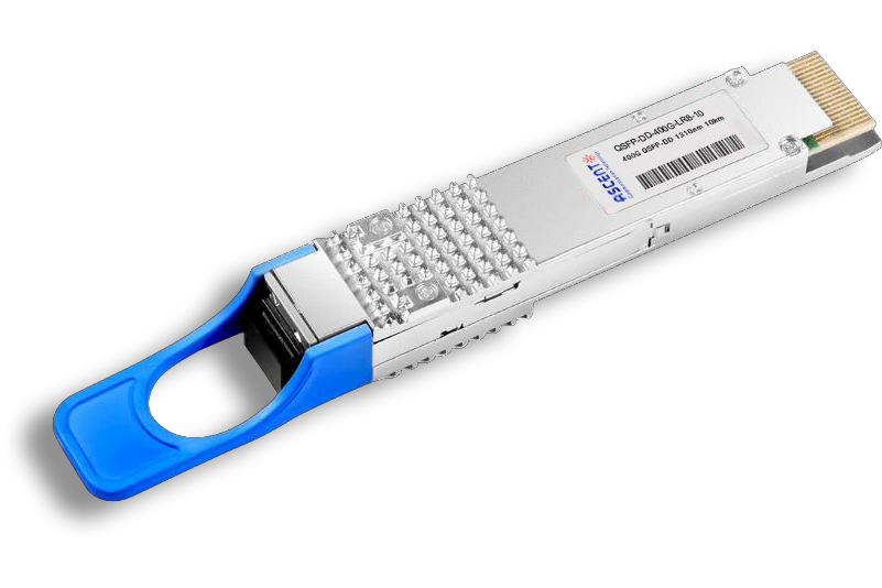
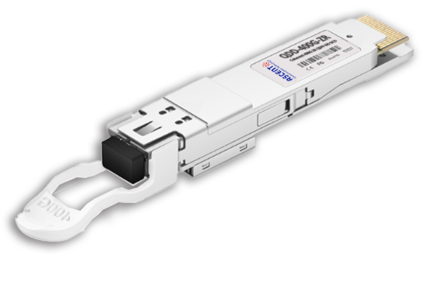
- FIBER OPTIC TRANSCEIVERS >800G & 400G Transceivers >400G QSFP56-DD 10km
400G QSFP56-DD 10km
The ACT QSFP56-DD 400Gb/s 4û100G LR1 optical module is designed for 10 km single-mode fiber (SMF) data-center and telecom interconnect applications. The module supports an aggregate data rate of 400 Gb/s by converting eight 53.125 Gb/s PAM4 electrical lanes into four parallel 100 Gb/s optical lanes, each operating in the 1310 nm wavelength range. On the receive side, the module converts four 100 Gb/s optical signals back into eight 53.125 Gb/s PAM4 electrical output lanes, enabling high-capacity bidirectional transmission. The optical interface uses a standard MPO-12 APC connector, with dedicated transmit and receive fiber lanes to support 4û100GBASE-LR1 operation. Accurate optical alignment is ensured by integrated guide pins within the receptacle. The electrical interface is compliant with the QSFP56-DD MSA edge connector, allowing seamless integration with QSFP-DD-based 400G network platforms. The module is fully compliant with the QSFP56-DD Multi-Source Agreement (MSA) Type 2 and supports CMIS 4.0 digital diagnostic monitoring, enabling real-time access to key operating parameters. Designed for reliable operation in data-center and telecom environments, the module meets stringent requirements for performance, signal integrity, and electromagnetic compatibility, ensuring stable operation across the specified commercial temperature range.
ôñ Breakout Mode
û4x100GBASE-LR1 compliant
106.25Gb/s with PAM4
û4x100GAUI-2 compliant
2x53.125Gb/s with PAM4
ôñ Or Aggregation Mode
û400 Gb/s Ethernet Protocol
4x106.25Gb/s with PAM4
û400GAUI-8 compliant
8x53.125Gb/s with PAM4
ôñ QSFP-DD MSA compliant
ôñ MPO-12 / APC connector with 8ô¯ angled end-face
ôñ Power consumption < 8W
ôñ Operating case temperature 0 to 70ô¯C
ôñ CMIS 4.0 management interface
Parameter | Symbol | Min. | Max. | Unit | Notes | |
Supply Voltage | VCC | 0 | 3.6 | V | ||
Storage Temperature | -40 | 85 | ô¯C | |||
Optical Receiver Input | - | 5.8 | dBm | Average, each lane | ||
Operating Conditions
Parameter | Symbol | Min. | Typ | Max. | Unit | Notes |
Supply Voltage | VCC | 3.135 | 3.3 | 3.465 | V | |
Supply Voltage Noise Tolerance | PSNRmod | - | - | 66 | mV | 10 Hz to 10 MHz |
Power Consumption | P_4 | - | - | 8 | W | |
Instantaneous Peak Current | Icc_ip_4 | 3200 | mA | |||
Sustained Peak Current | Icc-sp_4 | 2640.3 | mA | |||
Supply Current | Icc-4 | - | - | 2551.8 | mA | Steady state |
Case Temperature | TC | 0 | 25 | 70 | ô¯C |
Parameter | Symbol | Min. | Typ. | Max. | Unit | Notes |
Channel Data Rate | fDC | 106.25 | Gb/s | |||
Signaling Rate | fSG | 106.25 | Gb/s | PAM4 | ||
Signal Speed Variation from Nominal | ã¢fSG | -100 | +100 | ppm | ||
Wavelength (Range) | C | 1304.5 | 1317.5 | nm | ||
Side-Mode Suppression Ratio | SMSR | 30 | dB | |||
Average Launch Power | -1.9 | 4.8 | dBm | Note 1 | ||
Outer Optical Modulation Amplitude (OMAouter) | 1.1 | 5.0 | dBm | for TDECQ < 1.4 dB | ||
-0.3 + TDECQ | 5.0 | dBm | for 1.4 dB ãÊ TDECQ ãÊ 3.4 dB | |||
Transmitter and Dispersion Eye Closure for PAM4 | TDECQ | 3.4 | dB | |||
Transmitter Eye Closure for PAM4 | TECQ | 3.4 | dB | |||
| TDECQ ã TECQ | | 2.5 | dB | ||||
Over/Under-Shoot | 22 | % | ||||
Transmitter Power Excursion | 2.8 | dBm | ||||
Extinction Ratio | ER | 3.5 | dB | |||
Transmitter Transition Time | 17 | ps | ||||
Average Optical Output Power of Off Transmitter | Poff | -15 | dBm | |||
RIN15.6OMA | -136 | dB/Hz | ||||
Optical Return Loss Tolerance | 15.6 | dB | ||||
Transmitter Reflectance | -26 | dB | Note 2 | |||
Average Receive Power | -8.2 | 4.8 | dBm | Note 3 | ||
Receive Power (OMAouter) | 5.0 | dBm | ||||
Receiver Reflectance | -26 | dB | ||||
Receiver Sensitivity (OMAouter) | Max -6.1 | for TECQ<1.4 dB,Note 4 | ||||
Max (-7.5 + TECQ) | for 1.4 dB ãÊ TECQ ãÊ3.4 dB, Note 4 | |||||
Stressed Receiver Sensitivity (OMAouter) | -4.1 | dBm | Note 4, 5 | |||
Conditions of Stressed Receiver Sensitivity Test (Note 6) | ||||||
Stressed Eye Closure for PAM4 (SECQ), Lane under Test | SECQ | 3.4 | dB | |||
Notes:
1. Average launch power, each lane (min) is informative and not the principal indicator of signal strength. A transmitter with launch power below this value cannot be compliant; however, a value above this does not ensure compliance.
2. Transmitter reflectance is defined looking into the transmitter.
3. Average receive power, each lane (min) is informative and not the principal indicator of signal strength. A
received power below this value cannot be compliant; however, a value above this does not ensure compliance.
4. For when Pre-FEC BER is 2.4 x 10⁻⁴.
5. Measured with conformance test signal at TP3 (see IEEE Std 802.3-2022 clause 140.7.10) for the BER specified in IEEE Std 802.3-2022 clause 140.1.1.
6. These test conditions are for measuring stressed receiver sensitivity. They are not characteristics of the receiver. 
RX_LOS Characteristics
Parameter | Symbol | Min. | Typ. | Max. | Unit | Notes |
Receiver Loss of Signal Indicator Assert Level | RX_LOS | -15 | - | -9.6 | dBm | Average power |
Receiver Loss of Signal Indicator De-assert Level | RX_LOS | - | - | -9.1 | dBm | Average power |
Hysteresis | RX_LOS | 0.5 | - | - | dB |
Electrical Characteristics
Parameter | Min. | Typ. | Max. | Unit | Notes |
Module Output (each Lane, at TP4) [Note 1] | |||||
Signaling Rate per Lane (Range) | -100ppm | 53.125 | +100ppm | Gb/s | |
AC Common-Mode Output Voltage(RMS) | - | - | 17.5 | mV | |
Differential Peak-to-Peak Output Voltage | - | - | 900 | mV | |
Near-End ESMW (Eye Symmetry Mask Width) | 0.265 | - | - | UI | |
Near-End Eye Height, Differential | 70 | - | - | mV | |
Far-End ESMW (Eye Symmetry Mask Width) | 0.2 | - | - | UI | |
Far-End Eye Height, Differential | 30 | - | - | mV | |
Far-End Pre-Cursor ISI Ratio | -4.5 | - | 2.5 | % | |
Differential Output Return Loss | Equation (83E-2) | - | - | dB | Note 2 |
Common to Differential Mode Conversion Return Loss | Equation (83E-3) | - | - | dB | Note 2 |
Differential Termination Mismatch | - | - | 10 | % | |
Transition Time (Min, 20% to 80%) | 9.5 | - | - | ps | |
DC Common Mode Voltage | -350 | - | 2850 | mV | |
Module Input (each Lane) | |||||
Signaling Rate per Lane (Range) | -100ppm | 53.125 | +100ppm | Gb/s | |
Differential Pk-Pk Input Voltage Tolerance | 900 | - | - | mV | at TP1a |
Differential Input Return Loss | Equation (83E-5) | - | - | dB | at TP1, Note 2 |
Differential to Common Mode Input Return Loss | Equation (83E-6) | - | - | dB | at TP1, Note 2 |
Differential Termination Mismatch | - | - | 10 | % | at TP1 |
ESMW (Eye Symmetry Mask Width) | 0.22 | - | - | UI | at TP1a |
Eye Width | 0.22 | - | - | UI | at TP1a |
Applied Pk-Pk Sinusoidal Jitter | Table 120Eã6 | MHz, UI | at TP1a | ||
Eye Height | 32 | - | - | mV | at TP1a |
Single-ended input voltage tolerance range | -0.4 | - | 3.3 | V | at TP1a |
DC common mode voltage | -350 | - | 2850 | mV | at TP1 |
Notes:
1. Electrical module output is squelched for loss of optical input signal.
2. IEEE Std 802.3-2022 Section 6.

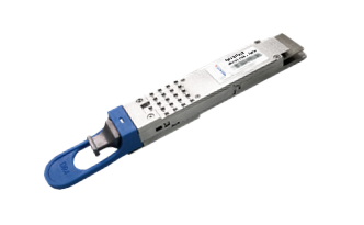
Pull tab color: Blue


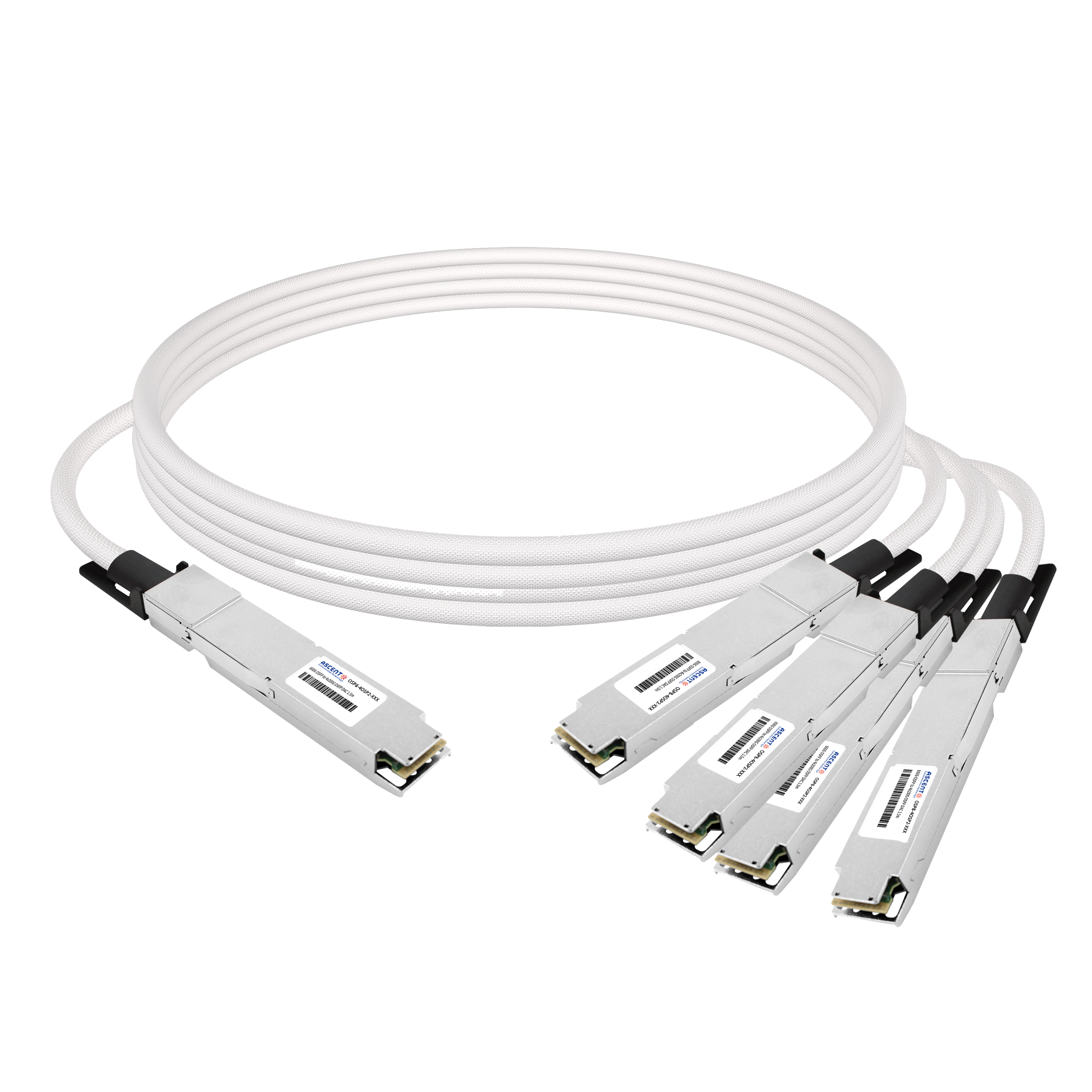
800G OSFP DAC Cable
800G IB NDR OSFP to 4xOSFP RHS Hairtail+ Direct Attach Copper Cable
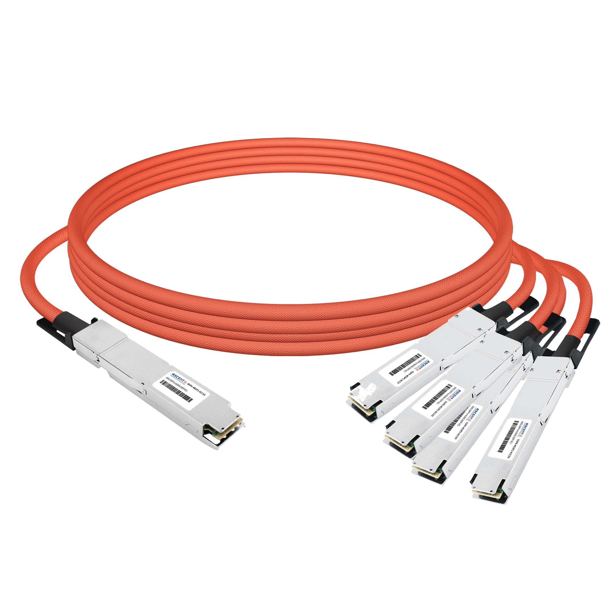
800G OSFP ACC Cable
800G OSFP Breakout to 4x200G OSFP Active Copper Cable
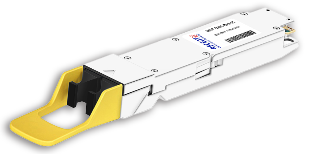
800G OSFP DR8 1310 nm 500 m
800 Gb/s DR8 OSFP 500m Optical Transceiver
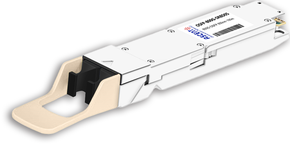
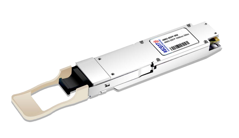
800G OSFP SR8 850 nm 100 m
OSFP-800G-SR8D-01 800 Gb/s OSFP SR8 850 nm 100 m Transceiver
400G QSFP-DD ZR+
QSFP-DD-ZR-80 400 Gb/s QSFP-DD 80 km Transceiver
400G QSFP-DD ER8 40 km
QSFP-DD-ER8-40 400 Gb/s QSFP-DD 40 km Transceiver
400G QSFP-DD 40 km
400 Gb/s QSFP-DD 40 km Transceiver
400G QSFP-DD LR8 1310 nm 10 km
QSFP-DD-LR8-10 400 Gb/s QSFP-DD LR8 10 km Transceiver

400G QSFP-DD LR4 CWDM 10 km
QSFP-DD-LR4-10 400 Gb/s QSFP-DD LR4 CWDM 10 km Transceiver
400G QSFP-DD SR8 850 nm 100 m
QSFP-DD-LP-01 400 Gb/s QSFP-DD SR8 100 m Transceiver
400G QSFP-DD FR4 2km
400 Gb/s QSFP-DD FR4 2 km DDM Transceiver
400G QSFP-DD DR4 500m
400 Gb/s QSFP-DD DR4 500m Transceiver
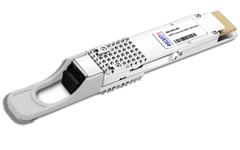
400G QSFP-DD DCO ZR
400G QSFP-DD DCO ZR Coherent Optical Transceiver
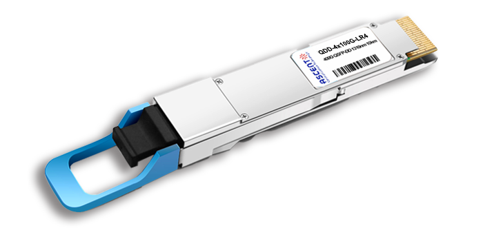
4X100G QSFP-DD LR4 10km
QDD 4x100G 1310nm LR 10 km Transceiver
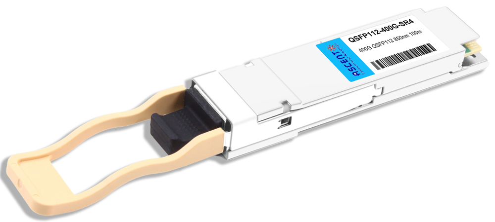
400G QSFP112 SR4 850 nm 100 m
QSFP112-400G-SR4-01 400 Gb/s QSFP112 SR4 850 nm 100 m Transceiver
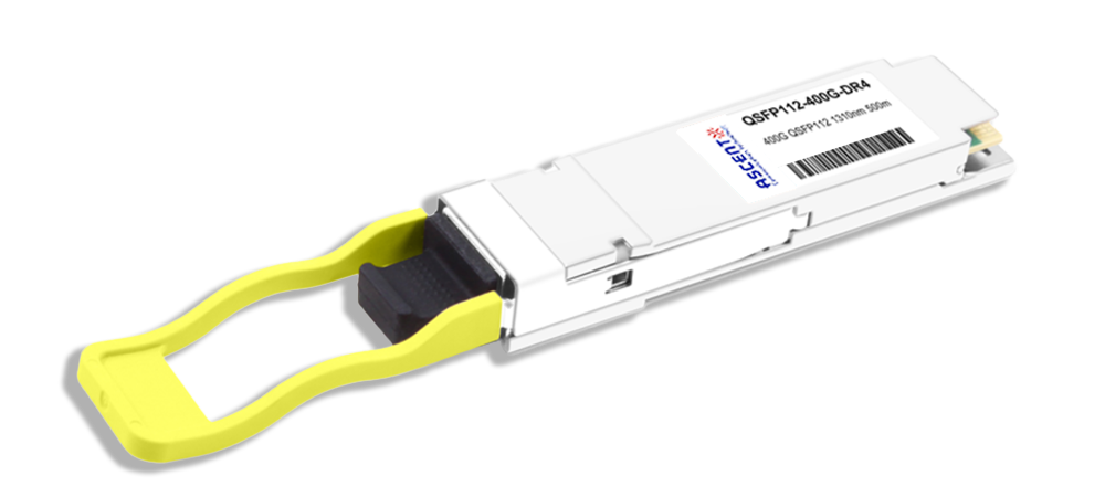
400G QSFP112 DR4 1310 nm 500 m
400G QSFP112 DR4 1310 nm Transceiver 500m
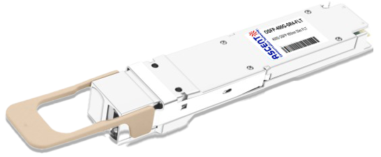
400G OSFP SR4 FLT 50m Transceiver
400 Gbps Multi-Mode 50m OSFP Transceiver
400G OSFP SR8 100m Transceiver
400 Gbps PSM8 Multi-Mode 100m OSFP Transceiver
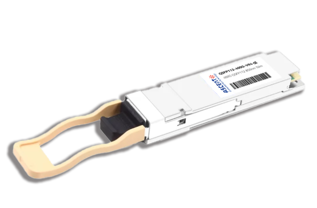
400G QSFP112 VR4 Transceiver
400G QSFP112 VR4
White Paper
Press Releases
Briefings 1
Briefings 2
Videos, etc.
QRG
Manual1
Manual2
Get in touch with our experts
Feedback