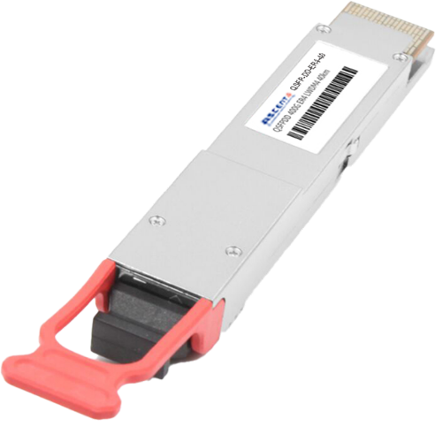
- FIBER OPTIC TRANSCEIVERS >800G & 400G Transceivers >400G QSFP-DD ER8 40 km
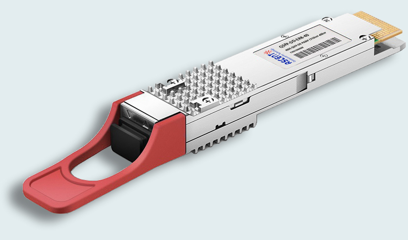
400G QSFP-DD ER8 40 km
Ascentãs QSFP-DD-ER8-40 is a 400 Gb/s Quad Small Form Factor Pluggable-double density (QSFP-DD) optical module designed for 40 km optical communication applications. It converts 8x 50G 400GAUI-8 PAM4 (Pulse-Amplitude Modulation) electrical input channels (each 53.125Gbps) into 8 Single Lambda 50G PAM4 LAN-WDM optical signals which are multiplexed for transmission over single fiber. On the receiver side, the optical signal is received and de-multiplexed and then QSFP-DD ER8 transceiver converts 8 Single Lambda 50G PAM4 LAN-WDM optical signals into 8x 50G 400GAUI-8 electrical inputs.
ã Compliant with IEEE std 802.3cnTM-2019:
ã 400GBASE-ER8 optical interface
ã 400GAUI-8 electrical interface
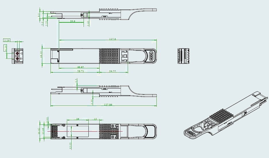
ã Compliant with QSFP-DD MSA HW Rev 5.1 with duplex LC connector
ã Compliant with QSFP-DD CMIS Rev 4.0
ã Case operating temperature 0ô¯C to 70ô¯C
ã Two wire serial Interface with digital diagnostic monitoring
ã Complies with EU Directive 2011/65/EU (RoHS compliant)
ã Class 1/1M Laser
Parameter | Symbol | Min. | Max. | Unit | Note |
Storage Temperature | TS | ã40 | 85 | ô¯C | |
Supply Voltage | VCC | ã0.5 | 3.6 | V | |
Relative Humidity (nonãcondensing) | RH | 5 | 95 | % | Nonãcondensing |
Data Input Voltage Differential | lVDIPãVDINl | ã | 1 | V | |
Control Input Voltage | VI | ã0.3 | VCC+0.5 | V | |
Control Output Voltage | VO | ã20 | 20 | V |
Recommended Operating Conditions
Parameter | Symbol | Min. | Typ. | Max. | Unit | Note |
Operating Case Temperature | TOPR | 0 | ã | 70 | ô¯C | |
Power Supply Voltage | VCC | 3.135 | 3.3 | 3.465 | V | |
Instantaneous Peak Current at Hot Plug | ICC_IP | ã | ã | 5600 | mA | |
Sustained Peak Current at Hot Plug | ICC_SP | ã | ã | 4620 | mA | |
Maximum Power Dissipation | PD | ã | ã | 14 | W | |
Maximum Power Dissipation, Low Power Mode | PDLP | ã | ã | 1.5 | W | |
Signaling Rate per Lane | SRL | ã | 26.5625 | ã | GBd | |
Control Input Voltage High | VIH | VCC*0.7 | ã | VCC+0.3 | ||
Control Input Voltage Low | VIL | ã0.3 | ã | VCC*0.3 | ||
Two Wire Serial Interface Clock Rate | ã | ã | ã | 400 | kHz | |
Power Supply Noise Tolerance | ã | ã | ã | 66 | mV | |
Rx Differential Data Output Load | ã | ã | 100 | ã | öˋ | |
Operating Distance | ã | 0.002 | ã | 40 | km | 1 |
Notes:
1. Channel insertion loss is 18 dB for 40 km
Transmitter Optical Characteristics
Parameter | Symbol | Min. | Typ. | Max. | Unit | Note |
Wavelength L0 | ö£C0 | 1272.55 | 1273.55 | 1274.54 | nm | |
Wavelength L1 | ö£C1 | 1276.89 | 1277.89 | 1278.89 | nm | |
Wavelength L2 | ö£C2 | 1281.25 | 1282.26 | 1283.27 | nm | |
Wavelength L3 | ö£C3 | 1285.65 | 1286.67 | 1287.68 | nm | |
Wavelength L4 | ö£C4 | 1294.53 | 1295.56 | 1296.59 | nm | |
Wavelength L5 | ö£C5 | 1299.02 | 1300.06 | 1301.09 | nm | |
Wavelength L6 | ö£C6 | 1303.54 | 1304.59 | 1305.63 | nm | |
Wavelength L7 | ö£C7 | 1308.09 | 1309.14 | 1310.19 | nm | |
Side Mode Suppression Ratio | SMSR | 30 | ã | ã | dB | |
Total Average Launch Power | AOPT | ã | ã | 14.6 | dBm | |
Average Launch Power, each Lane | AOPL | ã0.6 | ã | 5.6 | dBm | 1 |
Outer Optical Modulation Amplitude (OMAouter), each Lane | TOMA | 2.4 | ã | 6.4 | dBm | |
Difference in Launch Power between any Two Lanes (OMAouter) | DT_OMA | ã | ã | 4 | dB | |
Launch Power in OMAouter minus TDECQ, each Lane | TOMAãTDECQ | 1 | ã | ã | dBm | |
Transmitter and Dispersion Eye Closure for PAM4 (TDECQ), each Lane | TDECQ | ã | ã | 3.4 | dB | |
TDECQ ã10log10(Ceq) | ã | ã | ã | 3.4 | dB | |
Average Launch Power of OFF Transmitter, each Lane | TOFF | ã | ã | ã30 | dBm | |
Extinction Ratio | ER | 6 | ã | ã | dB | |
RIN15OMA | RIN | ã | ã | ã132 | dB/Hz | |
Optical Return Loss Tolerance | ORL | ã | ã | 15 | dB | |
Transmitter Reflectance | TR | ã | ã | ã26 | dB | 2 |
Notes:
1. Average launch power, each lane (min) is informative and not the principal indicator of signal strength
2. Transmitter reflectance is defined looking into the transmitter
Receiver Optical Characteristics
Parameter | Symbol | Min. | Typ. | Max. | Unit | Note |
Wavelength L0 | ö£C0 | 1272.55 | 1273.55 | 1274.54 | nm | |
Wavelength L1 | ö£C1 | 1276.89 | 1277.89 | 1278.89 | nm | |
Wavelength L2 | ö£C2 | 1281.25 | 1282.26 | 1283.27 | nm | |
Wavelength L3 | ö£C3 | 1285.65 | 1286.67 | 1287.68 | nm | |
Wavelength L4 | ö£C4 | 1294.53 | 1295.56 | 1296.59 | nm | |
Wavelength L5 | ö£C5 | 1299.02 | 1300.06 | 1301.09 | nm | |
Wavelength L6 | ö£C6 | 1303.54 | 1304.59 | 1305.63 | nm | |
Wavelength L7 | ö£C7 | 1308.09 | 1309.14 | 1310.19 | nm | |
Damage Threshold, each Lane | AOPD | ã3.4 | ã | ã | dBm | |
Average Receive Power, each Lane | AOPR | ã18.6 | ã | ã4.4 | dBm | |
Receive Power (OMAouter), each Lane | OMAR | ã | ã | ã3.6 | dBm | |
Difference in Receive Power between any Two Lanes (OMAouter) | DR_OMA | ã | ã | 5.8 | dB | |
Receiver Reflectance | RR | ã | ã | ã26 | dB | |
Receiver Sensitivity (OMAouter), each Lane | SOMA | ã | ã | Max(ã16.1, SECQ ã 17.5) | dBm | 1 |
Stressed Receiver Sensitivity (OMAouter), each Lane | SRS | ã | ã | ã14.1 | dBm | 2 |
Conditions of Stressed Receiver Sensitivity Test | ||||||
Stressed Eye Closure for PAM4 (SECQ), Lane Under Test | ã | ã | 3.4 | ã | dB | |
SECQ ã 10log10(Ceq), Lane Under Test | ã | 3.4 | dB | |||
OMAouter of each Aggressor Lane | ã | ã | ã8.3 | ã | dBm | |
Notes:
1. Receiver sensitivity (OMAouter), each lane (max) is informative and is defined for a transmitter with SECQ of 1.4 dB.
2. Measured with conformance test signal at TP3 for the BER = 2.4 x 10ã4
Electrical Specification High Speed Signal (Compliant with IEEE 802.3bs 400GAUIã8)
Parameter | Symbol | Min. | Typ. | Max. | Unit | Notes |
Receiver (Module Output) | ||||||
AC CommonãMode Output Voltage (RMS) | ã | ã | 17.5 | mV | ||
Differential Output Voltage | ã | ã | 900 | mV | ||
NearãEnd Eye Height, Differential | 70 | ã | ã | mV | ||
FarãEnd Eye Height, Differential | 30 | ã | ã | mV | ||
Far End PreãCursor Ratio | ã | ã | 2.5 | % | ||
Differential Termination Mismatch | ã | ã | 10 | % | ||
Transition Time (Min., 20% To 80%) | 9.5 | ã | ã | ps | ||
DC Common Mode Voltage | ã350 | ã | 2850 | mV | ||
Transmitter (Module Input) | ||||||
Differential pkãpk Input Voltage Tolerance | 900 | ã | ã | mV | ||
Differential Termination Mismatch | ã | ã | 10 | % | ||
SingleãEnded Voltage Tolerance Range | ã0.4 | ã | 3.3 | V | ||
DC Common Mode Voltage | ã350 | ã | 2850 | mV | ||
Electrical Specification Low Speed Signal (compliant with QSFPãDD HW Rev 5.1)
Parameter | Symbol | Min. | Max. | Unit | Note |
Module Output SCL and SDA | VOL | 0 | 0.4 | V | |
Module Input SCL and SDA | VIL | ã0.3 | VCC*0.3 | V | |
VIH | VCC*0.7 | VCC+0.5 | V | ||
InitMode, ResetL, and ModSelL | VIL | ã0.3 | 0.8 | V | |
VIH | 2 | VCC+0.3 | V | ||
IntL | VOL | 0 | 0.4 | V | |
VOH | VCCã0.5 | VCC+0.3 | V |
Timing for Soft Control and Status Functions
Parameter | Symbol | Min. | Max. | Unit | Note |
MgmtInit Duration | ã | 2000 | ms | ||
ResetL Assert Time | t_reset_init | 10 | ã | ôçs | |
IntL Assert Time | ton_IntL | ã | 200 | ms | |
IntL Deassert Time | toff_IntL | ã | 500 | ôçs | |
Rx LOS Assert Time | ton_losf | ã | 100 | ms | |
Flag Assert Time | ton_flag | ã | 200 | ms | |
Mask Assert Time | ton_mask | ã | 100 | ms | |
Mask Deassert Time | toff_mask | ã | 100 | ms | |
Module Select Wait Time | ModSelL Wait Time | ã | N/A | Not supported |
I/O Timing for Squelch and Disable
Parameter | Symbol | Min. | Max. | Unit | Notes |
Rx Squelch Assert Time | ton_Rxsq | ã | 50 | ms | |
Tx Squelch Assert Time | ton_Txsq | ã | 400 | ms | |
Tx Squelch Deassert Time | toff_Txsq | ã | 1500 | ms | Based on modulation |
Tx Disable Assert Time (fast mode) | ton_Txdisf | ã | 3 | ms | |
Tx Disable Deassert Time (fast mode) | toff_Txdisf | ã | 10 | ms | |
Rx Output Disable Assert Time | ton_Rxdis | ã | 100 | ms | |
Rx Output Disable Deassert Time | toff_Rxdis | ã | 100 | ms | |
Squelch Disable Assert Time | ton_sqdis | ã | N/A | ms | Not supported |
Squelch Disable Deassert Time | toff_sqdis | ã | N/A | ms | Not supported |
Digital Diagnostics
Parameter | Range | Accuracy | Unit | Calibration |
Temperature | 0 to 70 | ôÝ3 | ô¯C | Internal |
Voltage | 0 to VCC | 0.1 | V | Internal |
Tx Bias Current (Each Lane) | 0 to 100 | 10 % | mA | Internal |
Tx Output Power (Each Lane) | ã0.6 to +5.6 | ôÝ3 | dB | Internal |
Rx Receive Power (Each Lane) | ã18.6 to ã4.4 | ôÝ3 | dB | Internal |

800G OSFP DAC Cable
800G IB NDR OSFP to 4xOSFP RHS Hairtail+ Direct Attach Copper Cable
800G OSFP ACC Cable
800G OSFP Breakout to 4x200G OSFP Active Copper Cable
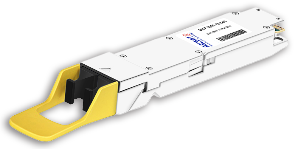
800G OSFP DR8 1310 nm 500 m
800 Gb/s DR8 OSFP 500m Optical Transceiver
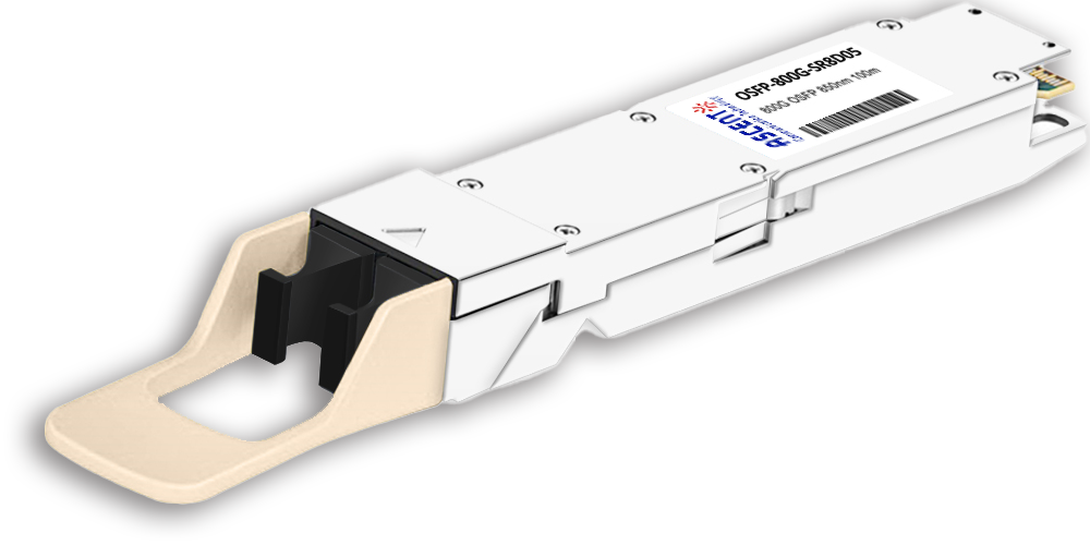
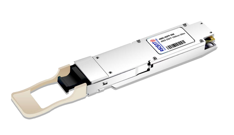
800G OSFP SR8 850 nm 100 m
OSFP-800G-SR8D-01 800 Gb/s OSFP SR8 850 nm 100 m Transceiver
400G QSFP56-DD 10km
400G QSFP-DD 4X100G LR1 Optical Transceiver
400G QSFP-DD ZR+
QSFP-DD-ZR-80 400 Gb/s QSFP-DD 80 km Transceiver
400G QSFP-DD 40 km
400 Gb/s QSFP-DD 40 km Transceiver
400G QSFP-DD LR8 1310 nm 10 km
QSFP-DD-LR8-10 400 Gb/s QSFP-DD LR8 10 km Transceiver

400G QSFP-DD LR4 CWDM 10 km
QSFP-DD-LR4-10 400 Gb/s QSFP-DD LR4 CWDM 10 km Transceiver
400G QSFP-DD SR8 850 nm 100 m
QSFP-DD-LP-01 400 Gb/s QSFP-DD SR8 100 m Transceiver
400G QSFP-DD FR4 2km
400 Gb/s QSFP-DD FR4 2 km DDM Transceiver
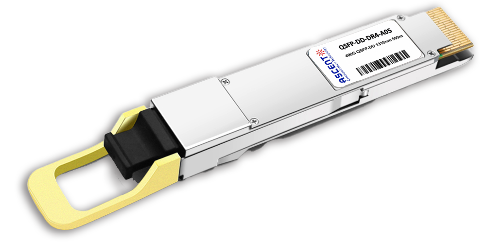
400G QSFP-DD DR4 500m
400 Gb/s QSFP-DD DR4 500m Transceiver
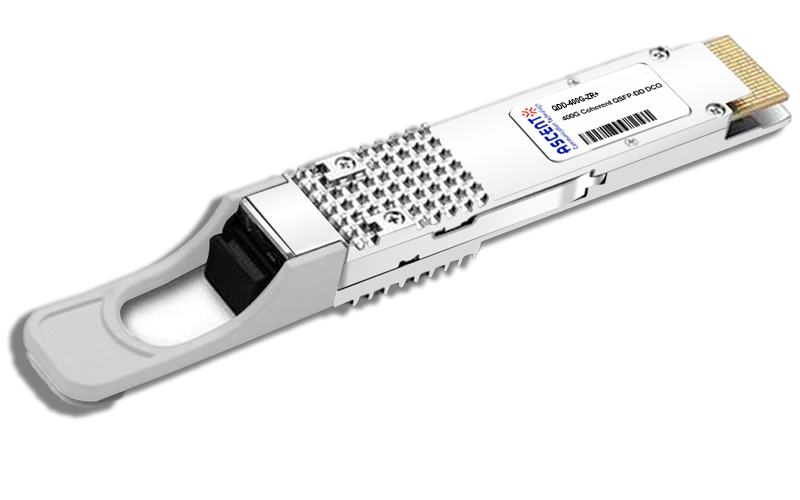
400G QSFP-DD DCO ZR
400G QSFP-DD DCO ZR Coherent Optical Transceiver
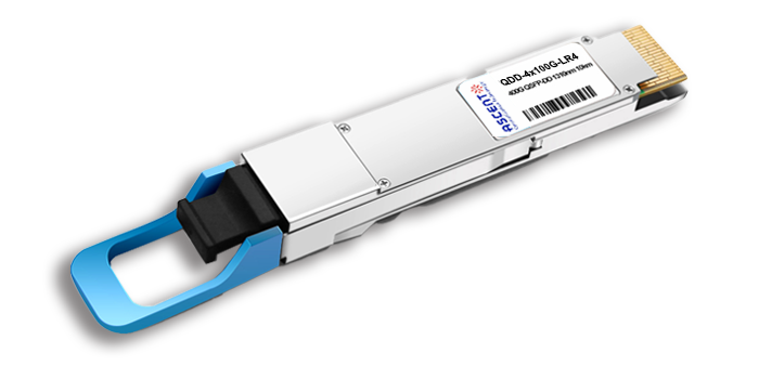
4X100G QSFP-DD LR4 10km
QDD 4x100G 1310nm LR 10 km Transceiver
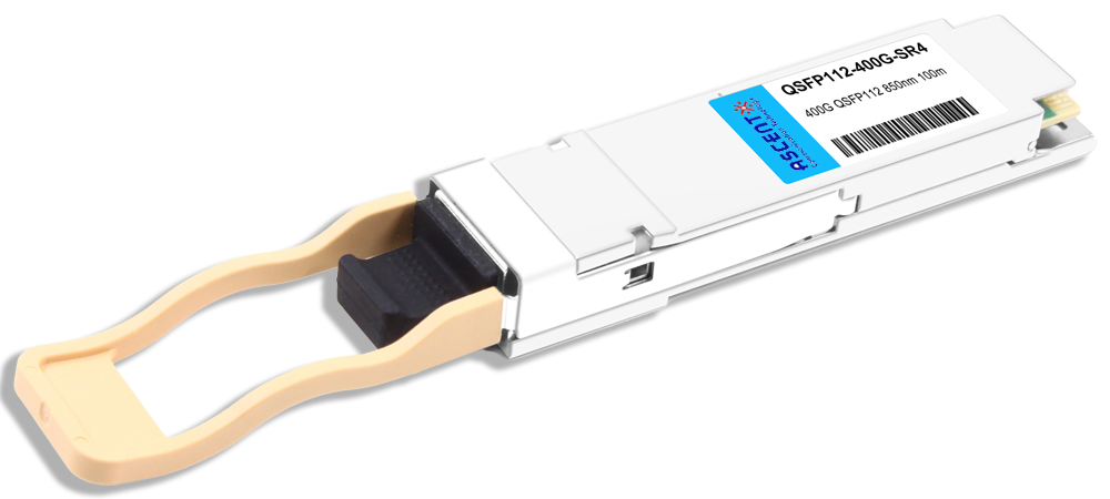
400G QSFP112 SR4 850 nm 100 m
QSFP112-400G-SR4-01 400 Gb/s QSFP112 SR4 850 nm 100 m Transceiver
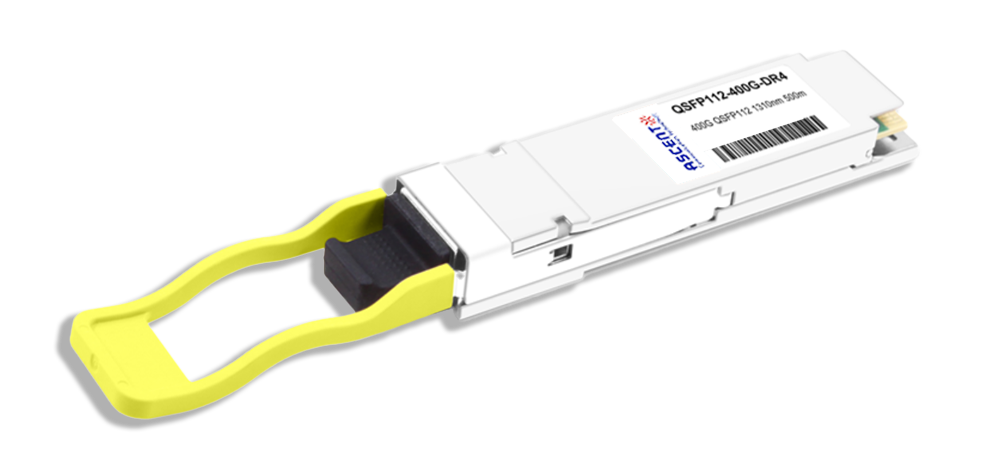
400G QSFP112 DR4 1310 nm 500 m
400G QSFP112 DR4 1310 nm Transceiver 500m
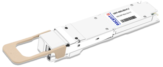
400G OSFP SR4 FLT 50m Transceiver
400 Gbps Multi-Mode 50m OSFP Transceiver
400G OSFP SR8 100m Transceiver
400 Gbps PSM8 Multi-Mode 100m OSFP Transceiver
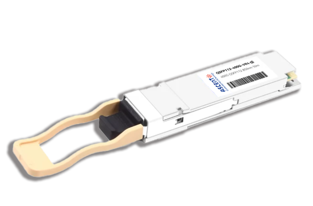
400G QSFP112 VR4 Transceiver
400G QSFP112 VR4
White Paper
Press Releases
Briefings 1
Briefings 2
Videos, etc.
QRG
Manual1
Manual2
Get in touch with our experts
Feedback