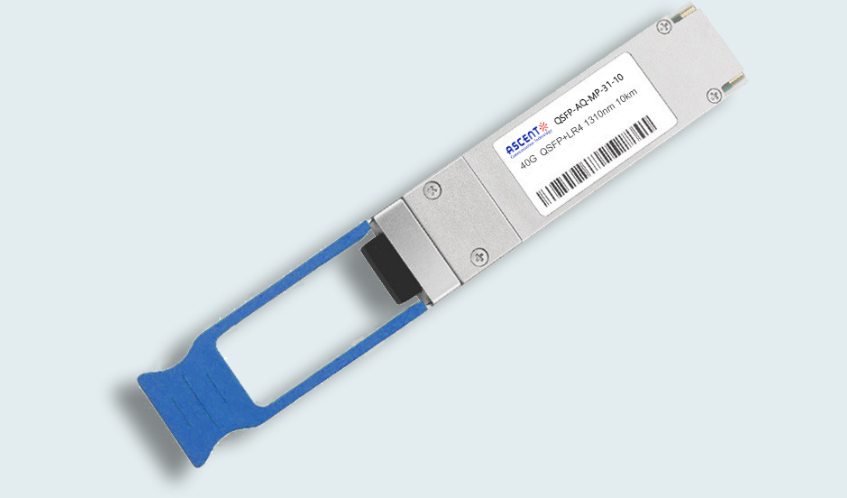
- FIBER OPTIC TRANSCEIVERS >40G & 25G Transceivers >40G QSFP+ LR4 10 km

40G QSFP+ LR4 10 km
Ascent QSFP+ LR4 is designed to operate over single-mode fiber system using 4X10 CWDM channel in 1310 band and links up to 10km. The module converts 4 inputs channel of 10Gb/s electrical data to 4 CWDM optical signals, and multiplexes them into a single channel for 40Gb/s optical transmission. Reversely, on the receiver side, the module optically de-multiplexes a 40Gb/s input into 4 CWDM channels signals, and converts them to 4 channel output electrical data. The central wavelengths of the 4 CWDM channels are 1271, 1291, 1311 and 1331 nm. It contains a duplex LC connector for the optical interface and a 38-pin connector for the electrical interface. Single-mode fiber (SMF) is applied in this module. This product converts the 4-channel 10Gb/s electrical input data into CWDM optical signals (light), by a 4-wavelength Distributed Feedback Laser (DFB) array. The 4 wavelengths are multiplexed into a single 40Gb/s data, propagating out of the transmitter module via the SMF. The receiver module accepts the 40Gb/s optical signals input, and de-multiplexes it into 4 CWDM 10Gb/s channels. Each wavelength light is collected by a discrete photo diode, and then outputted as electric data after amplified by a TIA. The product is designed with form factor, optical/electrical connection and digital diagnostic interface according to the QSFP+ Multi-Source Agreement (MSA) and compliant to 40G QSFP+ LR4 of IEEE 802.3ba.
ôñ Supports 41.2 Gb/s aggregate bitrates
ôñ Uncooled 4x10Gb/s transmitter
ôñ Maximum link length of 10km on Single Mode Fiber (SMF)
ôñ Hot-pluggable QSFP+ footprint
ôñ Duplex LC receptacles
ôñ Power consumption<3.5W
ôñ RoHS-6 compliant and lead-free
ôñ Single 3.3V power supply
ôñ Support Digital Diagnostic Monitor interface
ôñ Case operating temperature
Commercial: 0ô¯C to +70ô¯C
Absolute Maximum Ratings
Parameter | Symbol | Min. | Typ. | Max. | Unit | Note |
Storage Temperature | TS | -40 | 85 | ô¯C | ||
Storage Ambient Relative Humidity | HA | 0 | 85 | % | ||
Maximum Supply Voltage | VCC1, VCCTX, VCCRX | -0.5 | 3.6 | V | ||
Signal Input Voltage | -0.3 | Vcc+0.3 | V | |||
Receiver Damage Threshold | +3.4 | dBm | ||||
Lead Soldering Temperature/Time | TSOLD | 260/10 | ô¯C/sec | 1 | ||
Lead Soldering Temperature/Time | TSOLD | 360/10 | ô¯C/sec | 2 |
1. Suitable for wave soldering.
2. Only for soldering by iron.
General Product Characteristics
Parameter | Value | Unit | Note |
Module Form Factor | QSFP+ | ||
Number of Lanes | 4 Tx and 4 Rx | ||
Maximum Aggregate Data Rate | 41.2 | ||
Maximum Data Rate per Lane | 10.3125 | Higher bit rates may be supported. Please contact Ascent | |
Protocols Supported | Typical applications include 40G Ethernet | ||
Management Interface | Serial,I2c-based,400kHz maximum frequency | As defined by the QSFP+ MSA |
Parameter | Symbol | Min. | Typ. | Max. | Unit | Note |
Storage Temperature | BR | 10313 | Mb/s | 1 | ||
Storage Ambient Relative Humidity | BER | 10-12 | 2 | |||
Signal Input Voltage | d | 10 | km | 3 |
Notes:
1. Compliant with 40GBASE-LR4 and XLPPI per IEEE 802.3ba. Compatible with 1/10 Gigabit Ethernet and 1/2/4/8/10G Fibre Channel.
2. Tested with a PRBS 231-1 test pattern.
3. Per 40GBASE-LR4, IEEE 802.3ba.
Optical Parameters
Parameter | Symbol | Min. | Typ. | Max. | Unit |
Transmitter | |||||
Total Average Launch Power | POUT | 8.3 | dBm | ||
Average Output Power per lane | POUT | -7 | 2.3 | dBm | |
Transmit OMA per Lane | TxOMA | -4.0 | 3.5 | dBm | |
Extinction Ratio | ER | 3.5 | dB | ||
Center Wavelength | ö£C | 1264.5 | 1271 | 1277.5 | nm |
1284.5 | 1291 | 1297.5 | nm | ||
1304.5 | 1311 | 1317.5 | nm | ||
1324.5 | 1331 | 1337.5 | nm | ||
Side-mode Suppression Ratio | SMSR | 30 | - | - | dB |
Transmitter and Dispersion Penalty | TDP | 3.5 | dB | ||
Transmitter OFF Output Power | POff | -30 | dBm | ||
Transmitter Eye Mask Definition {X1, X2, X3, Y1, Y2, Y3} | {0.25, 0.4, 0.45, 0.25, 0.28, 0.4} | ||||
Receiver | |||||
Input Optical Wavelength | ö£IN | 1264.5 | 1271 | 1277.5 | nm |
1284.5 | 1291 | 1297.5 | nm | ||
1304.5 | 1311 | 1317.5 | nm | ||
1324.5 | 1331 | 1337.5 | nm | ||
Rx Sensitivity per lane | RSENS1 | -11.5 | dBm | ||
Rx Sensitivity(OMA) | RSENS2 | -9.6 | dBm | ||
InputSaturation Power (Overload) | PSAT | +3.4 | dBm | ||
Receiver Reflectance | Rfl | -12 | dBm | ||
Loss of Signal Assert | PA | -30 | dBm | ||
Loss of Signal De-assert | PD | -12.5 | dBm | ||
LOS Hysteresis | PD - PA | 0.5 | 6 | dB | |
Notes:
1. Even if TDP is<0.9dB, the OMA min must exceed this value.
Electrical Characteristics
Parameter | Symbol | Min. | Typ. | Max. | Unit | Note |
Supply Voltage | VCC1, | 3.15 | 3.45 | V | ||
VCCTX, | 3.15 | 3.45 | V | |||
VCCRX | 3.15 | 3.45 | V | |||
Transmitter | ||||||
Input different impedance | Rin | 90 | 100 | 110 | öˋ | 2 |
Single ended data input swing | Vin,pp | 120 | 820 | mV | ||
Transmitter Disable Voltage | VDIS | 2 | VCC | V | 3 | |
Transmitter Enable Voltage | VEN | 0 | 0.8 | V | ||
Data Dependent Input Jitter | DDJ | 0.3 | UI | |||
Receiver | ||||||
Output different impedance | Rout | 90 | 100 | 110 | öˋ | 2 |
Single ended data output swing | Vout,pp | 340 | 850 | mV | 4 | |
LOS Asserted | VLOSA | 2 | VCCHOST | V | 5 | |
LOS De-asserted | VLOSD | 0 | 0.8 | V | 5 | |
Power Supply Rejection | PSR | 50 | mVpp | |||
Notes:
1. Maximum total power value is specified across the full temperature and voltage range.
2. Connected directly to TX data input pins. AC coupled thereafter.
3. Or open circuit.
4. Into 100öˋ differential termination.
5. Loss of Signal is LVTTL. Logic ã0ãindicates normal operation; logic ã1ã indicates no signal detected.


64G SFP56 850nm 100m
64 Gb/s SFP56 SW Fibre Channel 850nm Transceiver
40/100G SFP28 SWDM4 100m
40/100Gb/s QSFP28, Bi-Di, Duplex LC 100m Transceiver

40G QSFP+ ER4 Industrial 40 km
40 Gb/s QSFP+ ER4 40 km Transceiver

40G QSFP+ ER4 40 km
40 Gb/s QSFP+ ER4 40 km Transceiver

40G QSFP+ LR4 Industrial 10 km
40 Gb/s QSFP+ LR4 10 km Transceiver

40G QSFP+ PSM4 2 km
40 Gb/s QSFP+ PSM4 Transceiver 2km
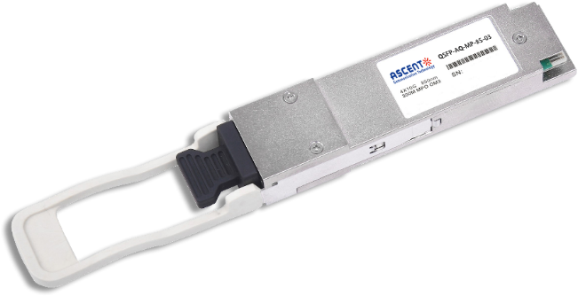
40G QSFP+ PLR4 1310 nm 10 km
QSFP-AQ-MP-31-10 40 Gb/s QSFP+ PSM 1310nm 10km MPO Optical Transceiver

40G QSFP+ CSR4 300m
40 Gb/s 300m QSFP+ CSR4 Transceiver
40GBASE-UNIV QSFP+ MMF and SMF
40G QSFP+ UNIV MMF/SMF 150m/2km
40G QSFP+ CWDM 2 km
40G QSFP+ CWDM 2 km
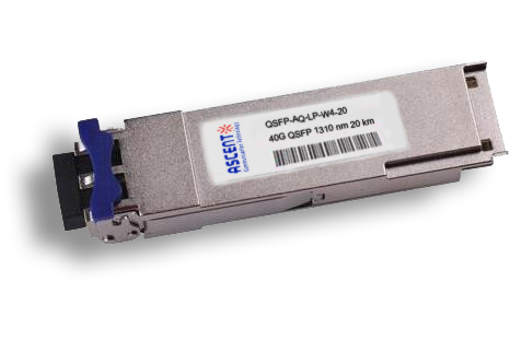
40G QSFP CWDM 20 km
QSFP-AQ-LP-W4-20 40 Gb/s QSFP CWDM 20 km Transceiver
40G QSFP+ SR4 300 m
40 Gb/s QSFP+ SR4 Transceiver with DDM
40G QSFP+ BIDI 150m
40 Gb/s QSFP+ BiDi Transceiver 150m
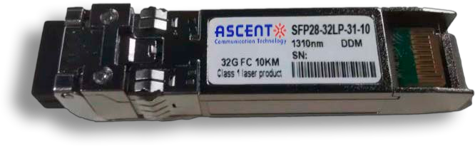
32G SFP28 1310 nm 10 km
32G FC 1310 nm 10 km SFP28 Transceiver

32G SFP28 SR 850 nm 100 m
SFP28-32LP-85-01 32GBASE-SR SFP28 850 nm 100 m DOM Transceiver
25G SFP28 BIDI 80 km
25G SFP28 BIDI 80 km Transceiver
.png)
25G SFP28 CWDM 10 km(E)
25 Gb/s CWDM EML SFP28 10 km Transceiver
25G SFP28 CWDM 10 km(D)
25 Gb/s CWDM SFP28 10 km Transceiver
25G SFP28 ZR 1310nm 80km
25 Gbps 1310 nm 80 km SFP28 ZR Transceiver
25G SFP28 1310 nm 40km
25 Gb/s 1310 nm Single-Mode SFP28 Transceiver
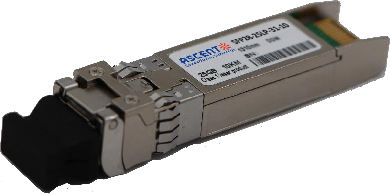
25G SFP28 1310 nm 10 km
SFP28-25LP-31-10 25 Gb/s 1310 nm Single-Mode SFP+ Transceiver
25G SFP28 850 nm 300m
25 Gb/s 850 nm Multi-Mode SFP28 300m Transceiver
25G SFP28 850 nm 100m
SFP28-25LP-85-01 28 Gb/s 850 nm Multi-Mode SFP28 Transceiver

10/25G SFP28 1310nm 40km
10/25 Gb/s SFP28 1310 nm 40km Transceiver
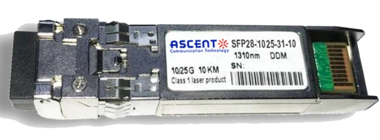
10/25G SFP28 1310nm 10km
10/25 Gb/s SFP28 1310 nm 10km DDM Transceiver

10/25G SFP28 850 nm 300m
10/25 Gb/s SFP28 850 nm 300m Transceiver

10/25G SFP28 850 nm 100m
10/25 Gb/s SFP28 850 nm 100m Transceiver
White Paper
Press Releases
Briefings 1
Briefings 2
Videos, etc.
QRG
Manual1
Manual2
Get in touch with our experts
Feedback