- FIBER OPTIC TRANSCEIVERS >40G & 25G Transceivers >40G QSFP+ ER4 40 km

40G QSFP+ ER4 40 km
Ascent QSFP+ ER4 is designed to operate over singlemode fiber system using 4 û 10 CWDM channels in 1310 band and links up to 40 km. The module converts 4 inputs channel of 10 Gb/s electrical data to 4 CWDM optical signals, and multiplexes them into a single channel for 40 Gb/s optical transmission. On the receiver side, the module optically de-multiplexes a 40 Gb/s input into 4 CWDM channels signals, and converts them to 4 output channels of electrical data. The central wavelengths of the 4 CWDM channels are 1271, 1291, 1311 and 1331 nm. It contains a duplex LC connector for the optical interface and a 38-pin connector for the electrical interface. Single-mode fiber (SMF) is applied in this module. This product converts the 4- channel 10 Gb/s electrical input data into CWDM optical signals (light), by a 4-wavelength Distributed Feedback Laser (DFB) array. The 4 wavelengths are multiplexed into a single 40 Gb/s data, propagating out of the transmitter module via the SMF. The receiver module accepts the 40Gb/s optical signals input, and de-multiplexes it into 4 CWDM 10 Gb/s channels. Each wavelength light is collected by a discrete photo diode, and then outputted as electric data after amplified by a TIA. The product is designed with form factor, optical / electrical connection and digital diagnostic interface according to the QSFP+ Multi-Source Agreement (MSA) and compliant to 40G QSFP+ ER4 of IEEE 802.3ba.
ôñ 4 CWDM lanes MUX/DEMUX design
ôñ Up to 11.2Gbps per channel bandwidth
ôñ Aggregate bandwidth of > 40Gbps
ôñ Duplex LC connector
ôñ Compliant with 40G Ethernet IEEE802.3ba and 40GBASE-ER4 Standard
ôñ QSFP MSA compliant
ôñ APD photo-detector
ôñ Up to 40km transmission
ôñ Compliant with QDR/DDR Infiniband data rates
ôñ Single +3.3V power supply operating
ôñ Built-in digital diagnostic functions
ôñ Temperature range 0ô¯C to 70ô¯C
ôñ RoHS Compliant Part
Absolute Maximum Ratings
Parameter | Symbol | Min. | Typ. | Max. | Unit | Note |
Storage Temperature | TS | -40 | +85 | ô¯C | ||
Supply Voltage | VCC | -0.5 | 4 | V | ||
Relative Humidity | RH | 0 | 85 | % |
Recommended Operating Conditions
Parameter | Symbol | Min. | Typ. | Max. | Unit | Note |
Case operating Temperature | TC | 0 | +70 | ô¯C | ||
Supply Voltage | VCCT, R | +3.13 | 3.3 | +3.47 | V | |
Supply Current | ICC | 1000 | mA | |||
Power Consumption | PD | 3.5 | W |
Electrical Characteristics (TOP = 0 to 70 ô¯C, VCC = 3.13 to 3.47 Volts)
Parameter | Symbol | Min. | Typ. | Max. | Unit | Note |
Data Rate per Channel | - | 10.3125 | 11.2 | Gbps | ||
Power Consumption | - | 2.5 | 3.5 | W | ||
Supply Current | Icc | 0.75 | 1.0 | A | ||
Control I/O Voltage-High | VIH | 2.0 | Vcc | V | ||
Control I/O Voltage-Low | VIL | 0 | 0.7 | V | ||
Inter-Channel Skew | TSK | 150 | Ps | |||
RESETL Duration | 10 | Us | ||||
RESETL De-assert time | 100 | ms | ||||
Power On Time | 100 | ms | ||||
Transmitter | ||||||
Single Ended Output Voltage Tolerance | 0.3 | 4 | V | 1 | ||
Common Mode Voltage Tolerance | 15 | mV | ||||
Transmit Input Diff Voltage | VI | 150 | 1200 | mV | ||
Transmit Input Diff Impedance | ZIN | 85 | 100 | 115 | ||
Data Dependent Input Jitter | DDJ | 0.3 | UI | |||
Receiver | ||||||
Single Ended Output Voltage Tolerance Rx Output Diff Voltage | 0.3 | 4 | V | |||
Vo | 370 | 600 | 950 | mV | ||
Rx Output Rise and Fall Voltage | Tr/Tf | 35 | ps | 1 | ||
Total Jitter | TJ | 0.3 | UI | |||
1. 20 to 80%
Optical Parameters (TOP = 0 to 70 ô¯C, VCC = 3.0 to 3.6 Volts)
Parameter | Symbol | Min. | Typ. | Max. | Unit | Note |
Transmitter | ||||||
Wavelength Assignment | L0 | 1264.5 | 1271 | 1277.5 | nm | |
L1 | 1284.5 | 1291 | 1297.5 | nm | ||
L2 | 1304.5 | 1311 | 1317.5 | nm | ||
L3 | 1324.5 | 1331 | 1337.5 | nm | ||
Side-mode Suppression Ratio | SMSR | 30 | - | - | dB | |
Total Average Launch Power | PT | - | - | 8.3 | dBm | |
Average Launch Power, each Lane | -1 | - | 5 | dBm | ||
TDP, each Lane | TDP | 2.3 | dB | |||
Extinction Ratio | ER | 5 | 6.0 | dB | ||
Transmitter Eye Mask Definition {X1, X2, X3, Y1, Y2, Y3} | {0.25, 0.4, 0.45, 0.25, 0.28, 0.4} | |||||
Optical Return Loss Tolerance | - | - | 20 | dB | ||
Average Launch Power OFF Transmitter, each Lane | Poff | -30 | dBm | |||
Relative Intensity Noise | Rin | -128 | dB/HZ | 1 | ||
Optical Return Loss Tolerance | - | - | 12 | dB | ||
Receiver | ||||||
Damage Threshold | THd | 3 | dBm | 1 | ||
Average Power at Receiver Input, each Lane | R | -21 | -6 | dBm | ||
Receive Electrical 3 Db Upper Cut off Frequency, each Lane | 12.3 | GHz | ||||
RSSI Accuracy | -2 | 2 | dB | |||
Receiver Reflectance | Rrx | -26 | dB | |||
Receive Electrical 3 dB upper Cutoff Frequency, each Lane | - | - | 3.5 | GHz | ||
LOS De-Assert | LOSD | -25 | dBm | |||
LOS Assert | LOSA | -35 | dBm | |||
LOS Hysteresis | LOSH | 0.5 | dB |
Notes:
1. 12dB Reflection.


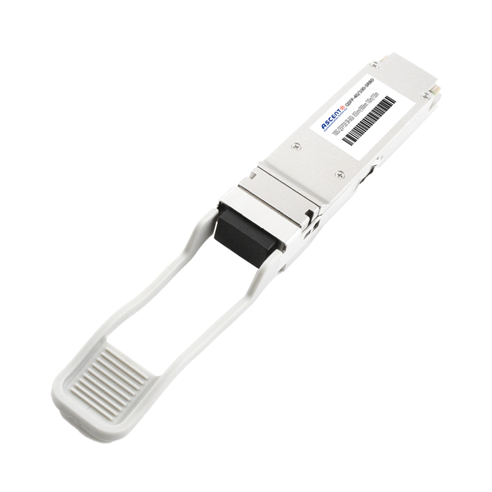
64G SFP56 850nm 100m
64 Gb/s SFP56 SW Fibre Channel 850nm Transceiver
40/100G SFP28 SWDM4 100m
40/100Gb/s QSFP28, Bi-Di, Duplex LC 100m Transceiver

40G QSFP+ ER4 Industrial 40 km
40 Gb/s QSFP+ ER4 40 km Transceiver

40G QSFP+ LR4 Industrial 10 km
40 Gb/s QSFP+ LR4 10 km Transceiver

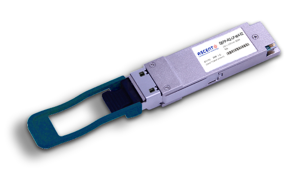
40G QSFP+ LR4 10 km
QSFP-AQ-LP-W4-10 40 Gb/s QSFP LR4 10 km Transceiver

40G QSFP+ PSM4 2 km
40 Gb/s QSFP+ PSM4 Transceiver 2km
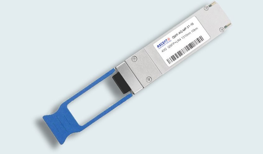
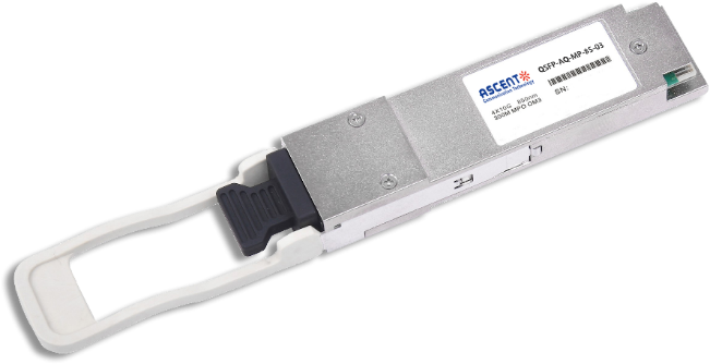
40G QSFP+ PLR4 1310 nm 10 km
QSFP-AQ-MP-31-10 40 Gb/s QSFP+ PSM 1310nm 10km MPO Optical Transceiver

40G QSFP+ CSR4 300m
40 Gb/s 300m QSFP+ CSR4 Transceiver
40GBASE-UNIV QSFP+ MMF and SMF
40G QSFP+ UNIV MMF/SMF 150m/2km
40G QSFP+ CWDM 2 km
40G QSFP+ CWDM 2 km
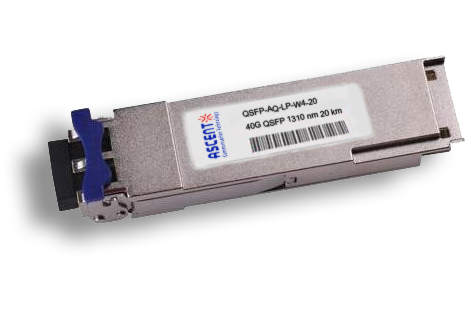
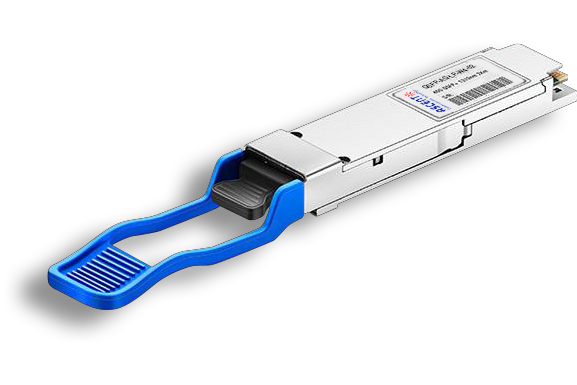
40G QSFP CWDM 20 km
QSFP-AQ-LP-W4-20 40 Gb/s QSFP CWDM 20 km Transceiver
40G QSFP+ SR4 300 m
40 Gb/s QSFP+ SR4 Transceiver with DDM
40G QSFP+ BIDI 150m
40 Gb/s QSFP+ BiDi Transceiver 150m
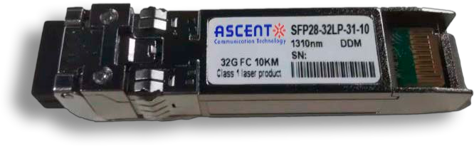
32G SFP28 1310 nm 10 km
32G FC 1310 nm 10 km SFP28 Transceiver

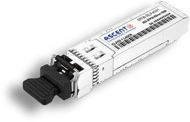
32G SFP28 SR 850 nm 100 m
SFP28-32LP-85-01 32GBASE-SR SFP28 850 nm 100 m DOM Transceiver
25G SFP28 BIDI 80 km
25G SFP28 BIDI 80 km Transceiver
.png)
25G SFP28 CWDM 10 km(E)
25 Gb/s CWDM EML SFP28 10 km Transceiver
25G SFP28 CWDM 10 km(D)
25 Gb/s CWDM SFP28 10 km Transceiver
25G SFP28 ZR 1310nm 80km
25 Gbps 1310 nm 80 km SFP28 ZR Transceiver
25G SFP28 1310 nm 40km
25 Gb/s 1310 nm Single-Mode SFP28 Transceiver
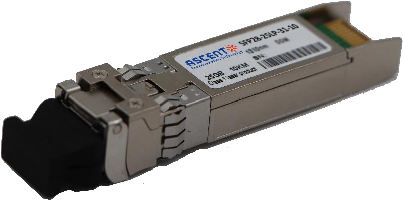
25G SFP28 1310 nm 10 km
SFP28-25LP-31-10 25 Gb/s 1310 nm Single-Mode SFP+ Transceiver
25G SFP28 850 nm 300m
25 Gb/s 850 nm Multi-Mode SFP28 300m Transceiver
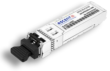
25G SFP28 850 nm 100m
SFP28-25LP-85-01 28 Gb/s 850 nm Multi-Mode SFP28 Transceiver

10/25G SFP28 1310nm 40km
10/25 Gb/s SFP28 1310 nm 40km Transceiver
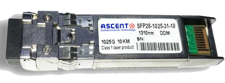
10/25G SFP28 1310nm 10km
10/25 Gb/s SFP28 1310 nm 10km DDM Transceiver

10/25G SFP28 850 nm 300m
10/25 Gb/s SFP28 850 nm 300m Transceiver

10/25G SFP28 850 nm 100m
10/25 Gb/s SFP28 850 nm 100m Transceiver
White Paper
Press Releases
Briefings 1
Briefings 2
Videos, etc.
QRG
Manual1
Manual2
Get in touch with our experts
Feedback