- FIBER OPTIC TRANSCEIVERS >40G & 25G Transceivers >40G QSFP+ SR4 150 m
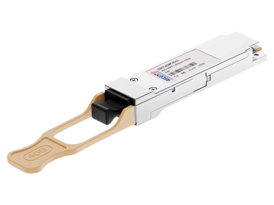
40G QSFP+ SR4 150 m
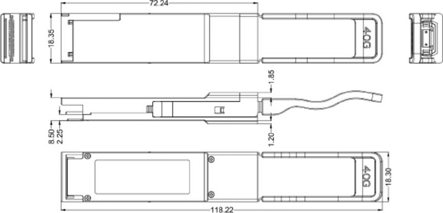
Ascent’s QSFP+ transceiver modules are designed for use in 40 Gigabit per second links over multimode fiber. They are compliant with the SFF-8436 and IEEE 802.3 40GBASE-SR4. Digital diagnostics functions are available via a I²C interface, including Tx and Rx power monitoring. The optical transceiver is compliant per the RoHS Directive 2011/65/EU. The optical transmitter portion of the transceiver incorporates a 4-channel VCSEL array, a 4-channel input buffer and laser driver, diagnostic monitors, control and bias blocks. For module control, the control interface incorporates a Two Wire Serial interface of clock and data signals. Diagnostic monitors for VCSEL bias, module temperature, transmitted optical power, received optical power and supply voltage are implemented and results are available through the TWS interface. Alarm and warning thresholds are established for the monitored attributes. Fault detection or channel deactivation through the TWS interface will disable the channel. Status, alarm/warning and fault information are available via the TWS interface. The optical receiver portion of the transceiver incorporates a 4-channel PIN photodiode array, a 4- channel TIA array, a 4-channel output buffer, diagnostic monitors, and control and bias blocks. Diagnostic monitors for optical input power are implemented and results are available through the TWS interface. Alarm and warning thresholds are established for the monitored attributes.
· Compliant with SFF-8436
· Compliant with IEEE 802.3 40GBASE-SR4
· 850nm 4 VCSEL Lasers and 4 channels PIN photo detectors
· Maximum link length of 100m on OM3 MMF or 150m on OM4 MMF
· 3.3V Supply Voltage
· Max. Power<1.5W
· 0-70°C Case Operating Temperature
· MPO Receptacle
· Maximum Data Rate per Lane: 10.3125Gb/s
· 2-wire interface for management and DDM
· Complies with EU Directive 2011/65/EU
· Class 1 Laser
Absolute Maximum Ratings
Parameter | Symbol | Min | Typ. | Max | Unit | Note |
Storage Temperature | Ts | -40 | - | +85 | °C | |
Relative Humidity (non-condensing) | RH | 5 | - | 95 | % | |
Supply Voltage | Vcc | -0.5 | - | 3.6 | V | |
Input Voltage | Vin | -0.5 | - | Vcc+0.5 | V |
Recommended Operating Conditions
Parameter | Symbol | Min | Typ. | Max | Unit | Note |
Operating Case Temperature | TOPR | 0 | - | 70 | °C | |
Power Supply Voltage | Vcc | 3.135 | 3.3 | 3.465 | V | |
Power Supply Current | Icc | 475 | mA | |||
Maximum Power Consumption | P_D | - | - | 1.5 | W | |
Data Rate per Lane | DR | - | 10.3125 | - | Gb/s | |
Operating Distance (MMF OM3) | - | 0.5 | - | 100 | m | |
Operating Distance (MMF OM5) | - | 0.5 | - | 150 | m |
Parameter | Symbol | Min | Typ. | Max | Unit | Note |
Transmitter | ||||||
Mean Wavelength (Each Lane) | λ | 840 | 850 | 860 | nm | |
Data Rate per Lane | DR | 10.3125 | Gbps | |||
Spectral Width (RMS) | Δλ | 0.65 | nm | |||
Optical Power (Each Lane) | POUT | -7.6 | - | 2.4 | dBm | |
OMA per Lane | Poma | -5.6 | 3 | dBm | ||
Peak Power, each Lane | P_peak | 4 | dBm | |||
Extinction Ratio | ER | 3 | dB | |||
TDP, each Lane | TDP | 3.5 | dB | |||
Optical Return Loss Tolerance | 12 | dB | ||||
Average Launch Power Tx_Off(Each Lane) | -30 | dBm | ||||
Receiver | ||||||
Wavelength(Each Lane) | λ | 840 | 850 | 860 | nm | |
Data rate per Lane | DR | 10.3125 | Gbps | |||
Average Power at Receiver, each Lane | - | -9.5 | - | 2.4 | dBm | |
Rx OMA per Lane | OMA | - | - | 3 | dBm | |
Stressed Receiver Sensitivity OMA (Each Lane) | SRS | - | - | -5.4 | dBm | |
Peak Power(Each lane) | - | - | - | 4 | dBm | |
Receiver Reflectance | RX_R | - | - | -12 | dB | |
LOS Assert | LOS_A | -30 | - | - | dBm | |
LOS De-Assert | LOS_D | - | - | -12 | dBm | |
LOS Hysteresis | - | 0.5 | - | dB | ||
Note: Measured with a PRBS 231-1 test pattern @10.3125Gbps, BER≤10-12.
High Speed Electrical Characteristics
Parameter | Symbol | Min | Typ. | Max | Unit | Note |
Supply Voltage | Vcc | 3.135 | 3.465 | V | ||
Supply Current | Icc | 450 | mA | |||
Input Differential Impedance | 90 | 100 | 110 | Ω | ||
Differential Data Input Swing | VIN, P-P | 300 | - | 1100 | mVpp | |
Differential Data Output Swing | Vout, P-P | 300 | 850 | mVpp | ||
Input Logic Level High | 2 | Vcc | ||||
Input Logic Level Low | 0 | 0.8 | ||||
Output Logic Level High | Vcc-0.5 | Vcc | ||||
Output Logic Level Low | 0 | 0.4 |
2-Wire Electrical Characteristics
Parameter | Symbol | Min | Typ. | Max | Unit | Note |
Host 2-Wire Vcc Voltage | Vcc_Host_2w | 3.14 | - | 3.46 | V | |
SCL and SDA Voltage | V_OL | 0 | - | 0.4 | V | |
V_OH | Vcc_Host_2w-0.5 | - | Vcc_Host_2w+0.3 | V | ||
V_IL | -0.3 | - | VccT*0.3 | V | ||
V_IH | VccT*0.7 | - | VccT+0.5 | V | ||
Input Current on the SCL and SDA Contacts | Ii | -10 | - | 10 | mA |
2-Wire Timing Characteristics
Parameter | Symbol | Min | Typ. | Max | Unit | Note |
Transmitter | ||||||
Clock Frequency | f_scl | 100 | 400 | kHZ | 1 | |
Clock Pulse Width Low | t_low | 1.3 | - | µs | ||
Clock Pulse Width High | t_high | 0.6 | - | µs | ||
Time Bus Free before New Transmission Can Start | t_buf | 20 | - | µs | 2 | |
START Hold Time | t_HD,STA | 0.6 | 0 | µs | ||
START Set-up Time | t_SU,STA | 0.6 | - | µs | ||
Data In Hold Time | t_HD,DAT | 0 | - | µs | ||
Data In Set-up Time | t_SU,DAT | 0.1 | - | µs | ||
Input Rise Time(100kHz) | tr,100 | - | 1000 | ns | 3 | |
Input Rise Time(400kHz) | tr,100 | - | 300 | ns | 3 | |
Input Fall Time(100kHz) | tf,100 | - | 300 | ns | 4 | |
Input Fall Time(400kHz) | tf,400 | - | 300 | ns | 4 | |
STOP Set-up Time | t_SU,STO | 0.6 | - | us | ||
Notes:
1. Module shall operate with fSCL up to 100 kHz without requiring clock stretching. The module may clock stretch with fSCL greater than 100 kHz and up to 400 kHz.
2. Between STOP and START and between ACK and ReSTART.
3. From (VIL,MAX-0.15) to (VIH,MIN+0.15).
4. From (VIH,MIN+0.15) to (VIL,MAX-0.15).
Memory Characteristics
Parameter | Symbol | Min | Typ. | Max | Unit | Note |
Serial Interface Clock Holdoff “Clock Stretching” | T_clock_hold | 500 | µs | 1 | ||
Complete Single or Sequential Write up to 4 Byte | tWR | 40 | ms | |||
Complete Sequential Write of 5 to 8 Byte | tWR | 80 | ms | |||
Endurance (Write Cycles) | 10K | - | - | ms |
Note: Maximum time the QSFP+ module may hold the SCL line low before continuing with a read or write operation.

64G SFP56 850nm 100m
64 Gb/s SFP56 SW Fibre Channel 850nm Transceiver
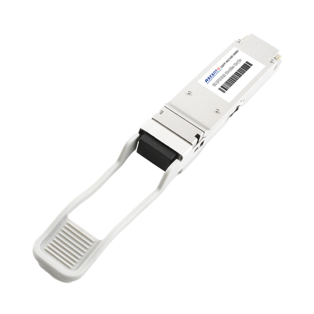
40/100G SFP28 SWDM4 100m
40/100Gb/s QSFP28, Bi-Di, Duplex LC 100m Transceiver

40G QSFP+ ER4 Industrial 40 km
40 Gb/s QSFP+ ER4 40 km Transceiver

40G QSFP+ ER4 40 km
40 Gb/s QSFP+ ER4 40 km Transceiver

40G QSFP+ LR4 Industrial 10 km
40 Gb/s QSFP+ LR4 10 km Transceiver

40G QSFP+ LR4 10 km
QSFP-AQ-LP-W4-10 40 Gb/s QSFP LR4 10 km Transceiver

40G QSFP+ PSM4 2 km
40 Gb/s QSFP+ PSM4 Transceiver 2km
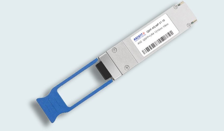
40G QSFP+ PLR4 1310 nm 10 km
QSFP-AQ-MP-31-10 40 Gb/s QSFP+ PSM 1310nm 10km MPO Optical Transceiver

40G QSFP+ CSR4 300m
40 Gb/s 300m QSFP+ CSR4 Transceiver
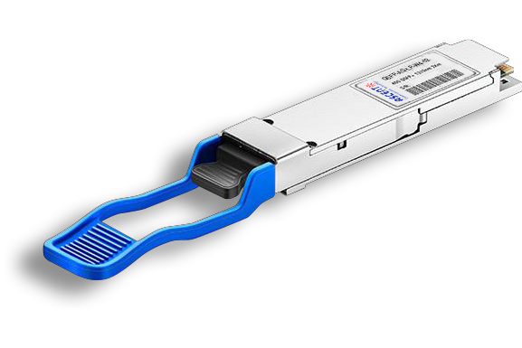
40GBASE-UNIV QSFP+ MMF and SMF
40G QSFP+ UNIV MMF/SMF 150m/2km
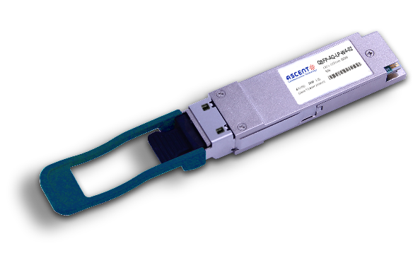
40G QSFP+ CWDM 2 km
40G QSFP+ CWDM 2 km
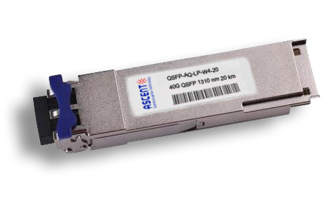
40G QSFP CWDM 20 km
QSFP-AQ-LP-W4-20 40 Gb/s QSFP CWDM 20 km Transceiver
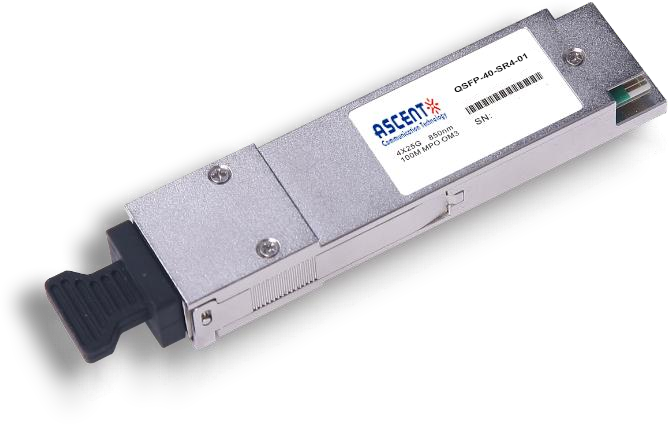
40G QSFP+ SR4 MPO 150 m
40 Gb/s 150m QSFP+ SR4 Transceiver with DDM
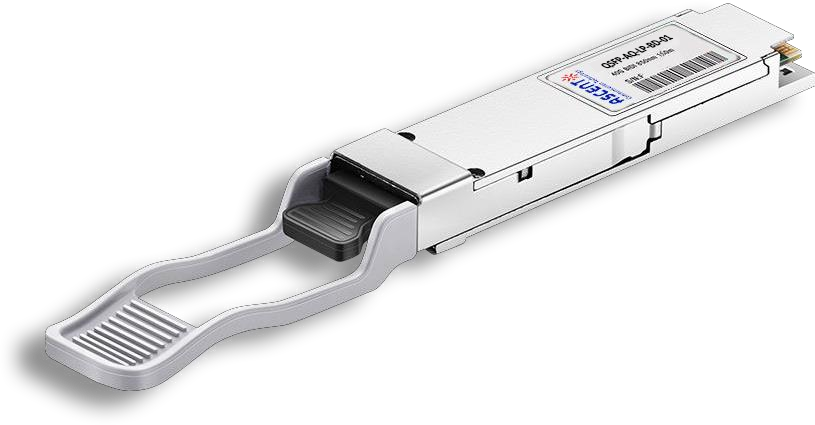
40G QSFP+ BIDI 150m
40 Gb/s QSFP+ BiDi Transceiver 150m
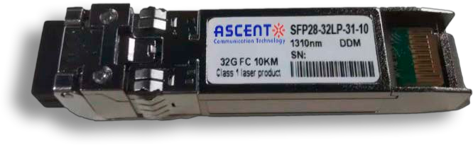
32G SFP28 1310 nm 10 km
32G FC 1310 nm 10 km SFP28 Transceiver

32G SFP28 SR 850 nm 100 m
SFP28-32LP-85-01 32GBASE-SR SFP28 850 nm 100 m DOM Transceiver
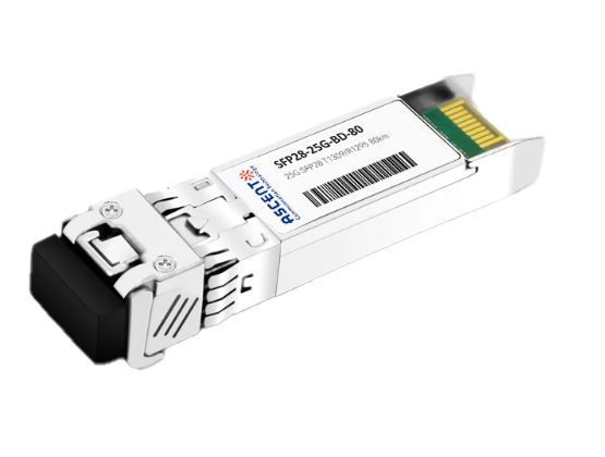
25G SFP28 BIDI 80 km
25G SFP28 BIDI 80 km Transceiver
.png)
25G SFP28 CWDM 10 km(E)
25 Gb/s CWDM EML SFP28 10 km Transceiver
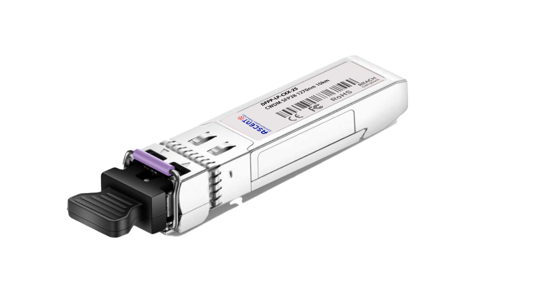
25G SFP28 CWDM 10 km(D)
25 Gb/s CWDM SFP28 10 km Transceiver
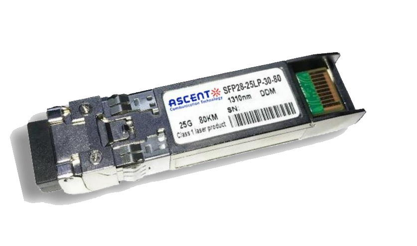
25G SFP28 ZR 1310nm 80km
25 Gbps 1310 nm 80 km SFP28 ZR Transceiver
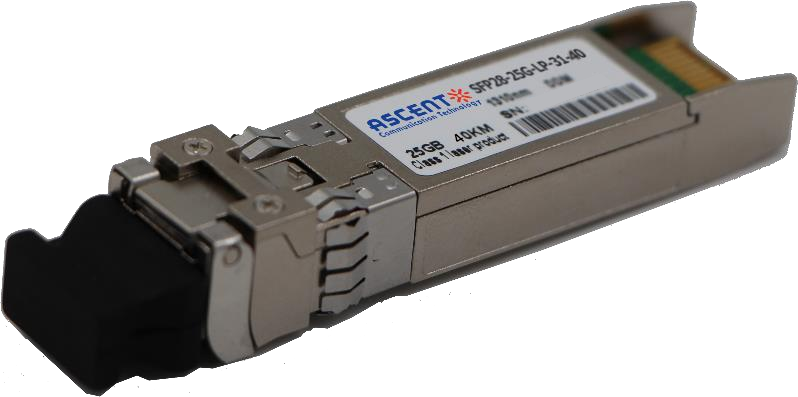
25G SFP28 1310 nm 40km
25 Gb/s 1310 nm Single-Mode SFP28 Transceiver
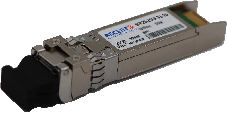
25G SFP28 1310 nm 10 km
SFP28-25LP-31-10 25 Gb/s 1310 nm Single-Mode SFP+ Transceiver
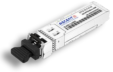
25G SFP28 850 nm 300m
25 Gb/s 850 nm Multi-Mode SFP28 300m Transceiver
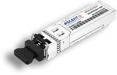
25G SFP28 850 nm 100m
SFP28-25LP-85-01 28 Gb/s 850 nm Multi-Mode SFP28 Transceiver
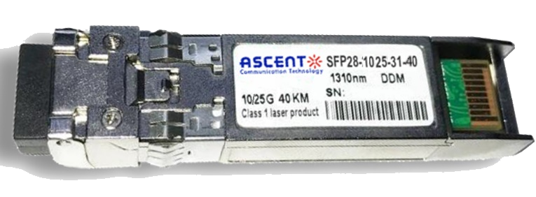
10/25G SFP28 1310nm 40km
10/25 Gb/s SFP28 1310 nm 40km Transceiver
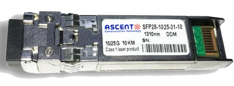
10/25G SFP28 1310nm 10km
10/25 Gb/s SFP28 1310 nm 10km DDM Transceiver

10/25G SFP28 850 nm 300m
10/25 Gb/s SFP28 850 nm 300m Transceiver

10/25G SFP28 850 nm 100m
10/25 Gb/s SFP28 850 nm 100m Transceiver
White Paper
Press Releases
Briefings 1
Briefings 2
Videos, etc.
QRG
Manual1
Manual2
Get in touch with our experts
Feedback