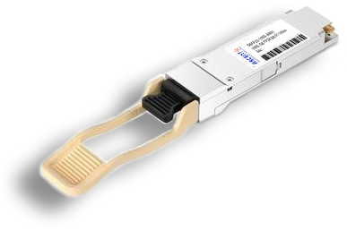
- FIBER OPTIC TRANSCEIVERS >200G & 100G Transceivers >100G QSFP28 DR Single ö£ 500 m
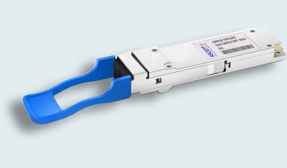
100G QSFP28 DR Single ö£ 500 m
Ascentãs QSFP28 100G DR1 Ethernet module is a transceiver module designed for 500m optical communication applications, and it is compliant with IEEE 802.3cu 100GBASE-DR standard.
ã Compliant with QSFP28 Standard SFF-8636 Rev 2.10a
ã Compliant with IEEE 802.3cd 100GBASE-DR
ã High speed I/O electrical interface (CAUI-4)
ã Single 3.3V Supply Voltage
ã Maximum power consumption 4W
ã 0-70 ô¤C Case Operating Temperature
ã 1310nm EML laser and PIN Receiver Array
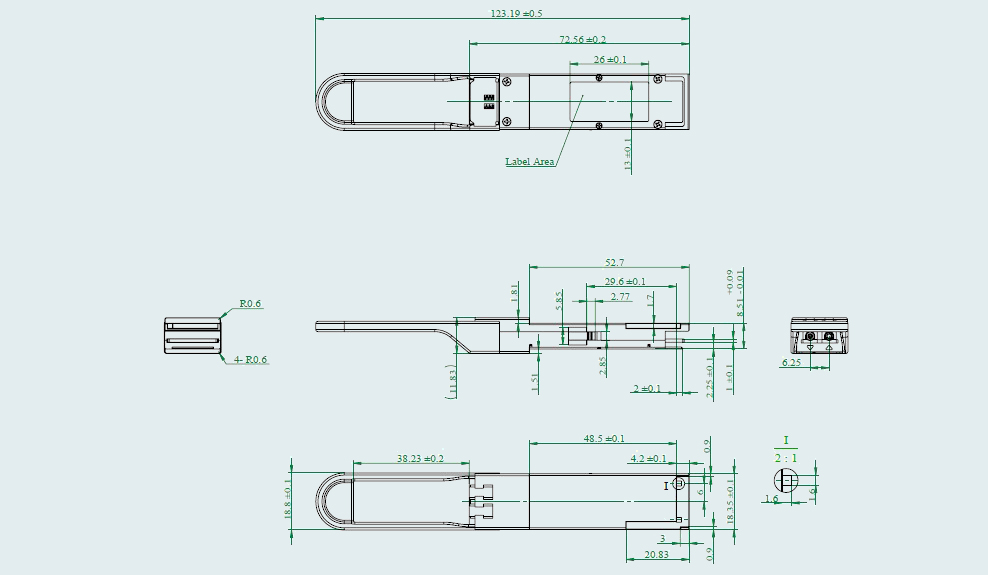
ã QSFP28 MSA package with duplex LC connector
ã Two Wire Serial Interface with Digital Diagnostic Monitoring
ã Complies with EU Directive 2011/65/EU (RoHS compliant)
ã Class 1 Laser
Absolute Maximum Ratings
Parameter | Symbol | Min. | Typ. | Max. | Unit | Note |
Storage Temperature | TS | ã40 | ã | +85 | ô¯C | |
Supply Voltage | VCC | ã0.3 | ã | 3.6 | V | |
Relative Humidity (nonãcondensing) | RH | 5 | ã | 95 | % | |
Data Input Voltage ã Differential | |VDIPãVDIN| | ã | ã | 1.0 | V | |
Control Input Voltage | VI | ã0.3 | ã | Vcc+0.5 | V | |
Control Output Current | IO | ã20 | ã | 20 | mA |
Recommended Operating Conditions
Parameter | Symbol | Min. | Typ. | Max. | Unit | Note |
Operating Case Temperature | TOPR | 0 | ã | 70 | ô¯C | |
Power Supply Voltage | VCC | 3.135 | 3.3 | 3.465 | V | |
Instantaneous Peak Current at Hot Plug | ICC_IP | ã | ã | 1600 | mA | |
Sustained Peak Current at Hot Plug | ICC_SP | ã | ã | 1320 | mA | |
Maximum Power Dissipation | PD | ã | ã | 4 | W | 1 |
Maximum Power Dissipation, Low Power Mode | PDLP | ã | ã | 1.5 | W | |
Signaling Rate | SR | ã | 53.125 | ã | GBd | |
Control Input Voltage High | VIH | VCC*0.7 | ã | VCC+0.3 | V | |
Control Input Voltage Low | VIL | ã0.3 | ã | VCC*0.3 | V | |
Two Wire Serial Interface Clock Rate | ã | ã | ã | 400 | kHz | |
Power Supply Noise | ã | ã | ã | 66 | mVpp | 2 |
Rx Differential Data Output Load | ã | ã | 100 | ã | ohms | |
Operating Distance | ã | 2 | ã | 500 | m |
Notes:
1. With power supply voltage 3.3V.
2. 10 Hz to 10 MHz.
Optical and Electrical Characteristics
Parameter | Symbol | Min. | Typ. | Max. | Unit | Note |
Transmitter | ||||||
Wavelength | ö£C | 1304.5 | 1311 | 1317.5 | nm | |
Side Mode Suppression Ratio | SMSR | 30 | ã | ã | dB | |
Average Optical Launch Power | POUT | ã2.9 | ã | 4 | dBm | |
Average Launch Power Tx_Off | POUT_OFF | ã | ã | ã15 | dBm | |
Extinction Ratio | ER | 3.5 | ã | ã | dB | |
Outer Optical Modulation Amplitude | OMAouter | ã0.8 | ã | 4.2 | dBm | |
Launch Power in OMAouter Minus TDECQ for ER ãË 4.5dB | OMAouterã TDECQ | ã2.2 | ã | ã |
dBm | |
Launch Power in OMAouter Minus TDECQ for ER < 4.5dB | OMAouterã TDECQ | ã1.9 | ã | ã |
dBm | |
Transmitter and Dispersion Eye Closure | TDECQ | ã | ã | 3.4 | dB | |
TDECQ ã 10*log10(Ceq) | ã | ã | 3.4 | dB | ||
Transmitter transition time | ã | ã | 17 | ps | ||
RIN17.1OMA | RIN | ã | ã | ã136 | dB/Hz | |
Optical return loss tolerance | ORLT | ã | ã | 15.5 | dB | |
Transmitter reflectance | TR | ã | ã | ã26 | dB | |
Receiver | ||||||
Wavelength | ö£C | 1304.5 | 1311 | 1317.5 | nm | |
Damage Threshold | 5 | ã | ã | dBm | ||
Average Receive Power | ã5.9 | ã | 4 | dBm | ||
Receive Power (OMAouter) | RP | ã | ã | 4.2 | dBm | |
Receiver Reflectance | RR | ã | ã | ã26 | dB | |
Receiver Sensitivity (OMAouter) | RS | max(ã3.9, SECQã5.3) |
dBm | |||
Stressed Receiver Sensitivity | SRS | ã | ã | ã1.9 | dBm | |
Stressed Receiver Sensitivity Test Conditions | ||||||
Stressed Eye Closure for PAM4 (SECQ) | SECQ | ã | 3.4 | ã | dB | |
SECQ ã 10*log10(Ceq) | ã | ã | 3.4 | dB | ||
Electrical Specifications
LowãSpeed Signal: Compliant to SFFã8679
HighãSpeed Signal: Compliant to CAUIã4 (IEEE 802.3ã2018)
Parameter | Symbol | Min. | Typ. | Max. | Unit | Notes |
Transmitter (Module Input) | ||||||
Differential Data Input Amplitude | VIN, PãP | 95 | ã | 900 | mVpp | 1 |
Differential Termination Mismatch | ã | ã | 10 | % | ||
LPMode, Reset and ModSelL | VIL | ã0.3 | ã | Vcc*0.3 | V | |
VIH | VCC*0.7 | ã | VCC+0.3 | V | ||
Receiver (Module Output) | ||||||
Differential Data Output Amplitude | VOUT, PãP | 250 | ã | 900 | mVpp | 1 |
Differential Termination Mismatch | ã | ã | 10 | % | ||
Output Rise/Fall Time, 20% to 80% | TR | 9.5 | ã | ã | ps | |
ModPrsL and IntL | VOL | 0 | ã | 0.4 | V | IOL = 4 mA |
VOH | VCCã0.5 | ã | VCC+0.3 | V | IOL = ã4 mA | |
Note 1: Amplitude customization beyond these specs is dependent on validation in customer system
Support for 100GAUIã4 at 26.5625 Gbd when using KP4 FEC in chipãtoãmodule interface.
Timing for QSFP28 Soft Control and Status Functions
Parameter | Symbol | Min. | Typ. | Max. | Unit | Note |
Initialization Time | t_init | ã | ã | 15 | s | 1 |
Reset Init Assert Time | t_reset_init | 10 | ã | ã | ôçs | |
Serial Bus Hardware Ready Time | t_serial | ã | ã | 2000 | ms | |
Monitor Data Ready Time | t_data | ã | ã | 2000 | ms | |
Reset Assert Time | t_reset | ã | ã | 15 | s | 1 |
LPMode Assert Time | ton_LPMode | ã | ã | 100 | ôçs | |
LPMode Deãassert Time | toff_LPMode | ã | ã | 15 | s | 1 |
IntL Assert Time | ton_IntL | ã | ã | 200 | ms | |
IntL Deassert Time | toff_IntL | ã | ã | 500 | ôçs | |
Rx LOS Assert Time | ton_lol | ã | ã | 100 | ms | |
Tx Fault Assert Time | ton_Txfault | ã | ã | 200 | ms | |
Flag Assert Time | ton_flag | ã | ã | 200 | ms | |
Mask Assert Time | ton_mask | ã | ã | 100 | ms | |
Mask Deassert Time | toff_mask | ã | ã | 100 | ms | |
Application or Rate Select Change Time | t_ratesel | ã | ã | N/A | ms | 2 |
Power_overãride or Powerãset Assert Time | ton_Pdown | ã | ã | 100 | ms | |
Power_overãride or Powerãset Deãassert Time |
toff_Pdown |
ã |
ã |
15 |
s |
1 |
Notes:
1. DSP limitation.
2. This feature is unsupported.
I/O Timing for Squelch & Disable
Parameter | Symbol | Min. | Typ. | Max. | Unit | Note |
Rx Squelch Assert Time | ton_Rxsq | 500 | ms | 1 | ||
Rx Squelch Deassert Time | toff_Rxsq | 15 | s | 1 | ||
Tx Squelch Assert Time | ton_Txsq | 400 | ms | |||
Tx Squelch Deassert Time | toff_Txsq | 1500 | ms | 1 | ||
Tx Disable Assert Time | ton_txdis | 100 | ms | |||
Tx Disable Deassert Time | toff_txdis | 400 | ms | |||
Rx Output Disable Assert Time | ton_rxdis | 100 | ms | |||
Rx Output Disable Deassert Time | toff_rxdis | 100 | ms | |||
Squelch Disable Assert Time | ton_sqdis | 100 | ms | |||
Squelch Disable Deassert Time | toff_sqdis | 100 | ms |
Note 1: DSP limitation.
Digital Diagnostics
Parameter | Range | Accuracy | Unit | Calibration |
Temperature | 0 to 70 | ôÝ3 | ô¯C | Internal |
Voltage | 0 to VCC | 3 % | V | Internal |
Tx Bias Current (each Lane) | 0 to 100 | 10 % | mA | Internal |
Tx Output Power (each Lane) | ã2.4 to 4.0 | ôÝ3 | dB | Internal |
Rx Power (each Lane) | ã6.4 to 4.5 | ôÝ3 | dB | Internal |

200G QSFP DD LR4 10km
200 Gb/s QSFP DD LR4 10 km Transceiver
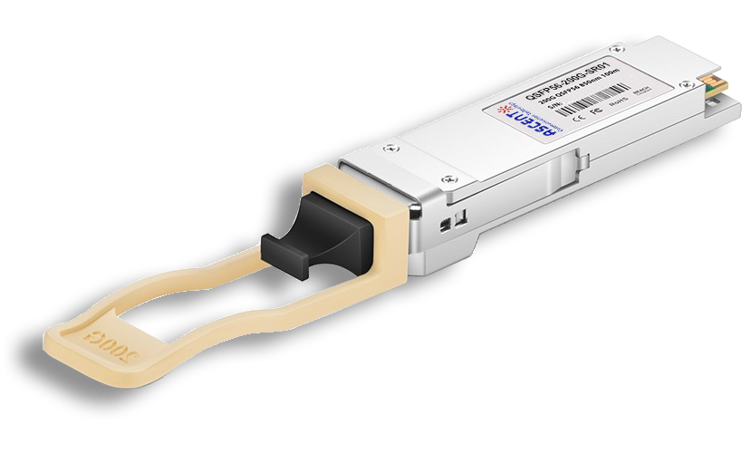
200G QSFP56 SR4 850 nm 100 m
QSFP56-200G-SR01 200 Gb/s QSFP56 SR4 850 nm 100 m Transceiver

100G QSFP28 LX4 2km
100 Gb/s 2km QSFP28 LX4 Transceiver

100G QSFP28OA LR4 10km
100 Gb/s 10 km QSFP28 LR4 Transceiver

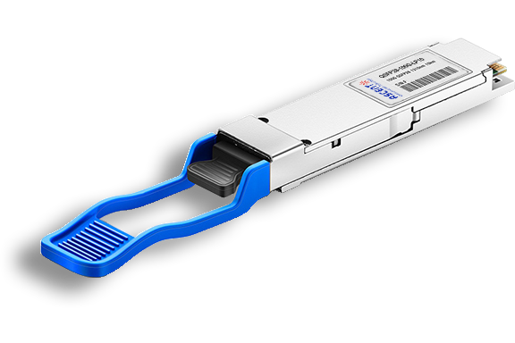
100G QSFP28 ZR4 1310 nm 80 km
QSFP28-100G-LP80 QSFP28 100 Gbps ZR4 Transceiver
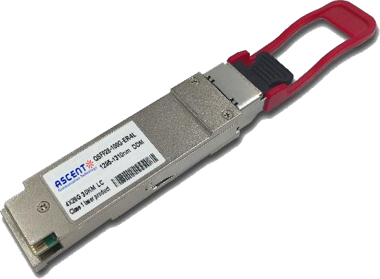
100G QSFP28 ER4L 1310 nm 40 km
QSFP28-100G-LP40 100 Gb/s 40 km QSFP28 ER4 Lite Transceiver

100G QSFP28 ER4 1310 nm 40 km
100 Gb/s 40 km QSFP28 ER4 Transceiver
100G QSFP28 LR4 1310 nm 10 km
QSFP28-100G-LP10 100 Gb/s 10km QSFP28 LR4 Transceiver

100G QSFP28 LR Single ö£ 10 km
100G QSFP28 LR1 10 km Single Channel

100G QSFP28 DR Single ö£ 500 m
QSFP28 100G DR Single Lambda Transceiver
100G QSFP28 CWDM4 1310 nm 2 km
QSFP28-100G-LP02 QSFP28 100 Gbps CWDM4 Transceiver
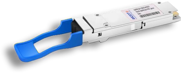
100G QSFP28 PSM4 1310 nm 2 km
QSFP28-100G-PSM4 100 Gb/s 1310 nm 2 km Transceiver
100G QSFP28 SR4 850 nm 100 m
QSFP28-100G-SR01 100 Gb/s SR4 850 nm 100 m Transceiver
100G QSFP28 FR Single ö£ 1310 nm 2 km
100G QSFP28 FR 2km Transceiver

100G QSFP28 SR01 BIDI MMF 850nm 100m
QSFP28 BIDI 100 Gb/s SR Transceiver 100m

100G QSFP28 BIDI 80km
QSFP28 BIDI 100 Gb/s ZR4 Transceiver 80km

100G QSFP28 BIDI 40km
QSFP28 BIDI 100 Gb/s ER Transceiver 40km

100G QSFP28 EZR4 100km
QSFP28 100Gb/s EZR4 Transceiver 100km

100G SFP56 ER1 30km
SFP56-DD 100G-ER1 Optical Transceiver 30km

100G SFP56 LR1 10km
SFP56-DD 100G-LR1 Optical Transceiver 10km
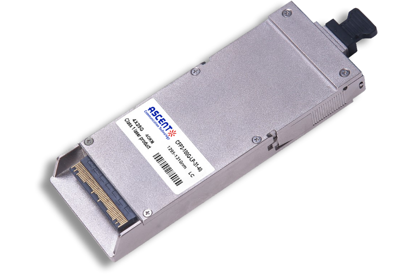
100G CFP2 ER4 40 km
CFP2-LP-31-40 100 Gb/s CFP2 ER4 40 km Transceiver
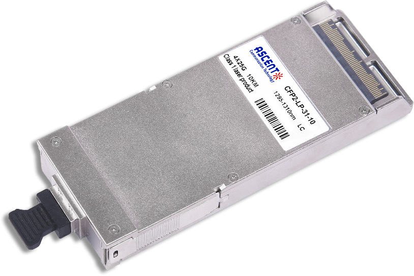
100G CFP2 LR4 10 km
CFP2-LP-31-10 100 Gb/s CFP2 LR4 10 km Transceiver
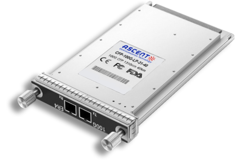
100G CFP ER4 40 km
CFP-LP-31-40 100 Gb/s CFP ER4 40 km Transceiver
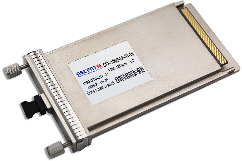
100G CFP LR4 10 km
CFP-LP-31-10 100 Gb/s CFP LR4 10 km Transceiver
White Paper
Press Releases
Briefings 1
Briefings 2
Videos, etc.
QRG
Manual1
Manual2
Get in touch with our experts
Feedback