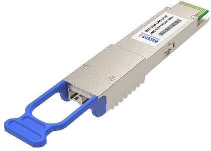
The Q28-100G-BD-LU80/LD80 is a 100Gbps BIDI QSFP28 ZR4 lite transceiver, designed for extended-range applications with up to 80 km of 100GBase-BX throughput over single-mode fiber (SMF) using LC connectors. Its robust design enables reliable high-speed connectivity for data centers, storage area networks, and 100G Ethernet. This transceiver operates bidirectionally, supporting two wavelength configurations. The Q28-100G-BD-LD80 transmits at 1295.56, 1300.05, 1304.58, and 1309.14nm, while the Q28-100G-BD-LU80 transmits at 1273.54, 1277.89, 1282.26, and 1286.66nm, both with complementary reception wavelengths. For optimal use, it requires pairing with compatible devices of matching wavelengths. With digital diagnostics through its QSFP28 MSA-compliant I2C interface, the Q28-100G-BD-LU80/LD80 supports real-time monitoring of key parameters. Easy to install and hot-swappable, this transceiver is ideal for scalable, high-demand network environments, offering flexibility and reliability for long-distance data transmission.
· 4x25Gb/s LAN WDM Blue or Red Side TOSA, LAN WDM Red or Blue Side ROSA with SOA
· Support 100GBASE-ZR4 for line rate of 103.125Gbps and OTU4 for line rate of 111.81Gbps
· Compliant with IEEE 802.3-2012 Clause 88 standard IEEE 802.3bm CAUI-4 chip to module electrical standard ITU-T G.959.1-2012-02 standard
· Simplex LC connector
· Single +3.3V power supply operating
· Temperature range 0°C to 70°C
· RoHS Compliant Part
Parameter | Symbol | Min. | Typ. | Max. | Unit | Notes |
Storage Temperature | Ts | -40 | +85 | °C | ||
Supply Voltage | VccT, R | -0.5 | +4 | V | ||
Operating Relative Humidity | RH | 0 | +85 | % |
Parameter | Symbol | Min. | Typ. | Max. | Unit | Notes |
Operating Case Temperature | Tc | 0 | +70 | °C | ||
Power Supply Voltage | VccT, R | 3.13 | 3.3 | 3.47 | V | |
Power Supply Current | Icc | 1200 | 1800 | mA | ||
Maximum Power Consumption | PD | 6.5 | W |
Parameter | Symbol | Min. | Typ. | Max. | Unit | Notes |
Data Rate per Channel | - | 25.78125 | Gbps | |||
27.9525 | ||||||
Power Consumption | - | 4 | 6.5 | W | ||
Supply Current | Icc | 1.2 | 1.8 | A | ||
Control I/O Voltage-High | VIH | 2.0 | Vcc | V | ||
Control I/O Voltage-Low Inter-Channel Skew | VIL | 0 | 0.7 | V | ||
TSK | 35 | Ps | ||||
RESETL Duration | 10 | Us | ||||
RESETL De-assert time | 100 | ms | ||||
Power On Time | 100 | ms | ||||
Transmitter | ||||||
Single Ended Output Voltage Tolerance | 0.3 | Vcc | V | 1 | ||
Common mode Voltage Tolerance | 15 | mV | ||||
Transmit Input Diff Voltage | VI | 150 | 1200 | mV | ||
Transmit Input Diff Impedance | ZIN | 85 | 100 | 115 | ||
Data Dependent Input Jitter | DDJ | 0.3 | UI | |||
Receiver | ||||||
Single Ended Output Voltage Tolerance | 0.3 | 4 | V | |||
Rx Output Diff Voltage | Vo | 370 | 600 | 950 | mV | |
Rx Output Rise and Fall Voltage | Tr/Tf | 35 | ps | 1 | ||
Total Jitter | TJ | 0.3 | UI | |||
Optical Parameters (TOP = 0 to 70 °C, VCC = 3.0 to 3.6 Volts)
Parameter | Symbol | Min. | Typ. | Max. | Unit | Notes |
Transmitter(Module Input) | ||||||
Blue Side Four Lane Wavelength Range | 1 | 1272.54 | 1273.54 | 1274.54 | nm | |
2 | 1276.89 | 1277.89 | 1278.89 | nm | ||
3 | 1281.25 | 1282.26 | 1283.27 | nm | ||
4 | 1285.65 | 1286.66 | 1287.68 | nm | ||
Red Side Four Lane Wavelength Range | 1 | 1294.56 | 1295.56 | 1296.56 | nm | |
2 | 1299.05 | 1300.05 | 1301.05 | nm | ||
3 | 1303.58 | 1304.58 | 1305.58 | nm | ||
4 | 1308.14 | 1309.14 | 1310.14 | nm | ||
Side-mode Suppression Ratio | SMSR | 30 | - | - | dB | |
Total Average Launch Power | PT | 8 | - | 12.5 | dBm | |
Average Launch Power, each Lane | +2 | - | 6.5 | dBm | ||
Difference in Launch Power between any two Lanes (OMA) | - | - | 3 | dB | ||
Extinction Ratio | ER | 6 | - | - | dB | |
Transmitter Eye Mask Definition {X1, X2, X3, Y1, Y2, Y3} | {0.25, 0.4, 0.45, 0.25, 0.28, 0.4} | 1 | ||||
Optical Return Loss Tolerance | - | - | 20 | dB | ||
Average Launch Power OFF Transmitter, each Lane | Poff | -30 | dBm | |||
Relative Intensity Noise | Rin | -130 | dB/HZ | |||
Optical Return Loss Tolerance | 20 | dB | ||||
Transmitter Reflectance | - | - | 12 | dB | ||
Receiver | ||||||
Red Side Four Lane Wavelength Range | λ1 | 1272.54 | 1273.54 | 1274.54 | nm | |
λ2 | 1276.89 | 1277.89 | 1278.89 | nm | ||
λ3 | 1281.25 | 1282.26 | 1283.27 | nm | ||
λ4 | 1285.65 | 1286.66 | 1287.68 | nm | ||
Blue Side Four Lane Wavelength Range | λ1 λ2 | 1294.56 | 1295.56 | 1296.56 | nm | |
1299.05 | 1300.05 | 1301.05 | nm | |||
λ3 | 1303.58 | 1304.58 | 1305.58 | nm | ||
λ4 | 1308.14 | 1309.14 | 1310.14 | nm | ||
Total Damage Threshold | THd | 5.5 | dBm | 1 | ||
Receiver Sensitivity per Lane | R | -28 | dBm | |||
Average Power at Receiver Input, each Lane | R | -28 | 0 | dBm | 1 | |
LOS De-Assert | LOSD | -29 | dBm | |||
LOS Assert | LOSA | -40 | dBm | |||
LOS Hysteresis | LOSH | 0.5 | dB | |||
Parameter | Symbol | Max | Unit | Conditions |
Initialization Time | t_init | 2000 | ms | Time from power on1, hot plug or rising edge of Reset until the module is fully functional2 |
Reset Init Assert Time | t_reset_init | 2 | μs | A Reset is generated by a low level longer than the minimum reset pulse time present on the ResetL pin. |
Serial Bus Hardware Ready Time | t_serial | 2000 | ms | Time from power on1 until module responds to data transmission over the 2-wire serial bus |
Monitor Data Ready Time | t_data | 2000 | ms | Time from power on1 to data not ready, bit 0 of Byte 2, deasserted and IntL asserted |
Reset Assert Time | t_reset | 2000 | ms | Time from rising edge on the ResetL pin until the module is fully functional2 |
LPMode Assert Time | ton_LPMode | 100 | μs | Time from assertion of LPMode (Vin:LPMode =Vih) until module power consumption enters lower Power Level |
IntL Assert Time | ton_IntL | 200 | ms | Time from occurrence of condition triggering IntL until Vout:IntL = Vol |
IntL Deassert Time | toff_IntL | 500 | μs | toff_IntL 500 μs Time from clear on read3 operation of associated flag until Vout:IntL = Voh. This includes deassert times for Rx LOS, Tx Fault and other flag bits. |
Rx LOS Assert Time | ton_los | 100 | ms | Time from Rx LOS state to Rx LOS bit set and IntL asserted |
Flag Assert Time | ton_flag | 200 | ms | Time from occurrence of condition triggering flag to associated flag bit set and IntL asserted |
Mask Assert Time | ton_mask | 100 | ms | Time from mask bit set4 until associated IntL assertion is inhibited |
Mask De-assert Time | toff_mask | 100 | ms | Time from mask bit cleared4 until associated IntlL operation resumes |
ModSelL Assert Time | ton_ModSelL | 100 | μs | Time from assertion of ModSelL until module responds to data transmission over the 2-wire serial bus |
ModSelL Deassert Time | toff_ModSelL | 100 | μs | Time from deassertion of ModSelL until the module does not respond to data transmission over the 2-wire serial bus |
Power_over-ride or Power-set | ton_Pdown | 100 | ms | Time from P_Down bit set 4 until module power consumption enters lower Power Level |
Assert Time | ||||
Power_over-ride or Power-set | toff_Pdown | 300 | ms | Time from P_Down bit cleared4 until the module is fully functional3 |
De-assert Time |


200G QSFP DD LR4 10km
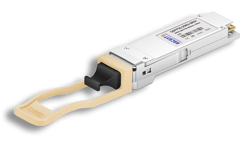
200G QSFP56 SR4 850 nm 100 m

100G QSFP28 LX4 2km

100G QSFP28OA LR4 10km

100G QSFP28 ZR4 1310 nm 80 km
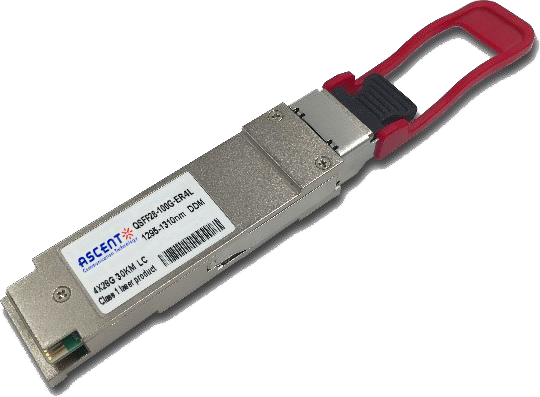
100G QSFP28 ER4L 1310 nm 40 km

100G QSFP28 ER4 1310 nm 40 km
100G QSFP28 LR4 1310 nm 10 km
100G QSFP28 LR Single λ 10 km

100G QSFP28 DR Single λ 500 m
100G QSFP28 CWDM4 1310 nm 2 km
100G QSFP28 PSM4 1310 nm 2 km
100G QSFP28 SR4 850 nm 100 m

100G QSFP28 FR Single λ 1310 nm 2 km

100G QSFP28 SR01 BIDI MMF 850nm 100m

100G QSFP28 BIDI 40km

100G QSFP28 EZR4 100km

100G SFP56 ER1 30km

100G SFP56 LR1 10km
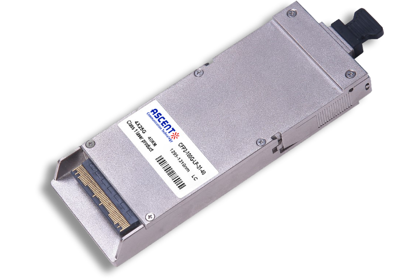
100G CFP2 ER4 40 km
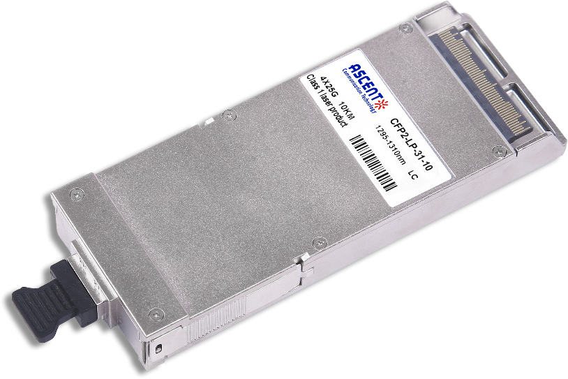
100G CFP2 LR4 10 km
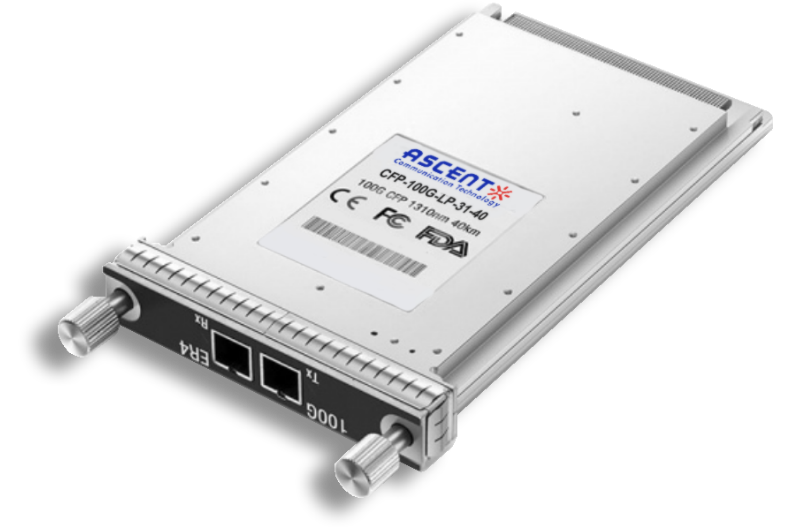
100G CFP ER4 40 km
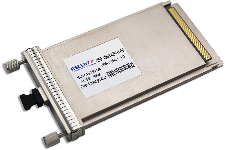
100G CFP LR4 10 km