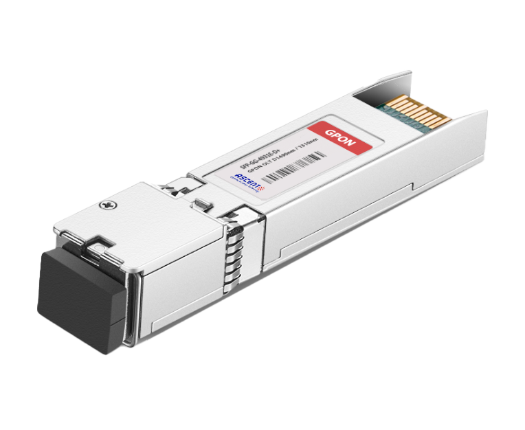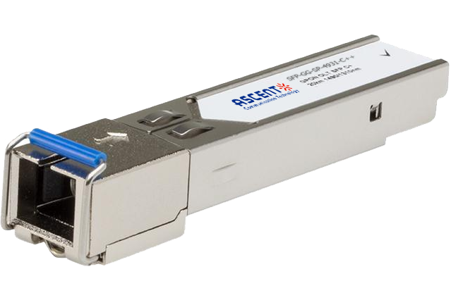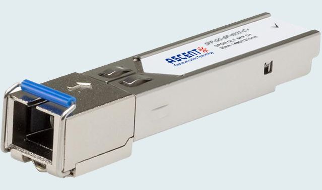
ASCENT’s GPON OLT transceiver SFP-GG-SP-4931 C+ is designed for optical line terminal (OLT) for ITU-T G.984.2 Class C+ requirements Network transmission. The optical transceiver is compliant with the Small Form- Factor Pluggable (SFP) Multi- Source Agreement (MSA). The GPON OLT SFP module is contained in a SFP package with SC/UPC receptacle connector. The module consists 1490 nm DFB laser, InGaAs APD, Preamplifier and WDM filter in a high-integrated optical sub-assembly, and it transmit up to 2.5 Gbps of continuous data at 1490 nm, and receives 1.25 Gbps burst-mode data at 1310 nm. The module data link up to 20 km in 9/125 µm single-mode fiber. Ascent GPON SFP is a low cost point to multi point (P2MP) Fiber to the Home, Business or Curb (FTTX) GPON OLT transceiver. It is fabricated with a rugged die cast metal housing and cage assembly. Commercial and industrial temperature ranges are available. It is IEC 60825-1 Class I laser safety compliant and meets the EEC Directive 2002/95/EC for RoHS compliance.
• Single-fiber bi-directional data links asymmetric TX 2488 Mbps / RX 1244 Mbps application
• Single fiber bi-directional data links asymmetric TX 2488Mbps/RX1244Mbps application
• 1490nm continuous-mode DFB laser transmitter and 1310nm burst-mode APD-TIA receiver
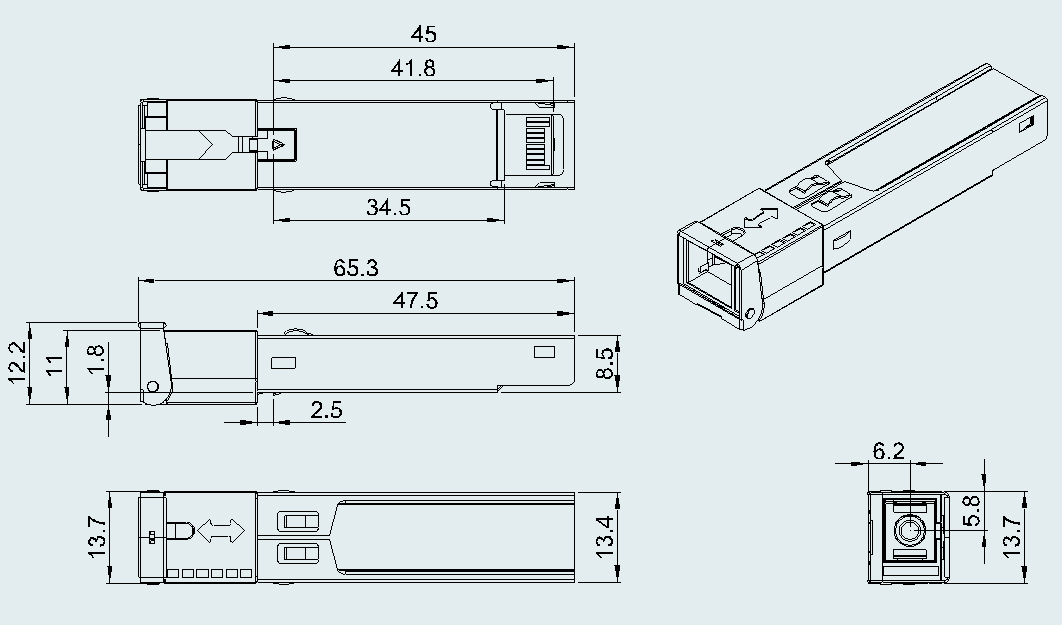
• Small Form Factor Pluggable package with SC/UPC Connector
• Single 3.3V power supply
• DDMI function available with internally calibrated mode
• Digital burst RSSI function to monitor the input optical power level
• LVPECL compatible data input/output interface
• LVTTL transmitter disable control
• LVTTL transmitter laser fault alarm
• Fast LVTTL receiver Signal Detect (SD) indication response
• Low EMI and excellent ESD protection
• International Class1 laser safety certified
• Operating temperature range:
Commercial: -5°C to 70°C
• Complies with EU Directive 2015/863/EU
• Complies with SFP Multi-Source Agreement (MSA) SFF-8074i
• Complies with ITU-T G.984.2 Amendment 1
• Complies with FCC 47 CFR Part 15, Class B
• Complies with FDA 21 CFR 1040.10 and 1040.11 except for deviations pursuant to Laser Notice No.
50, dated June 24, 2007
• Complies with SFF-8472
• Compatible with TR-NWT-000870 4.1 ESD sensitivity classification Class2
• Compatible with Telcordia GR-468-CORE
Absolute Maximum Ratings
Parameter | Symbol | Min. | Typ. | Max. | Unit | Notes |
Storage Ambient Temperature | TSTG | -40 | 85 | °C | ||
Storage Humidity | HS | 0 | 90 | °C | ||
Operating Humidity | Ho | 5 | 85 | % | ||
Power Supply Voltage | VCC | 0 | 3.6 | V | ||
Receiver Damaged Threshold | +4 | dBm |
Parameter | Symbol | Min. | Typ. | Max. | Unit | Notes |
Operating Case Temperature | TC | -5 | 70 | °C | ||
Power Supply Voltage | VCC | 3.13 | 3.3 | 3.47 | V | |
Power Consumption | PW | 1.65 | W | |||
Data Rate | TX 2.488 / RX 1.244 | Gbps |
Parameter | Symbol | Min. | Typ. | Max. | Unit | Notes |
Total Supply Current | ICC | 500 | mA | |||
Transmitter | ||||||
Transmitter Differential Input Voltage | 400 | 2400 | mV | |||
Tx_Fault Output Voltage - High | VOH | 2.4 | Vcc | V | LVTTL | |
Tx_Fault Output Voltage - Low | VOL | 0 | 0.4 | V | LVTTL | |
Tx_Disable Input Voltage - High | VIH | 2 | Vcc | V | LVTTL | |
Tx_Disable Input Voltage - Low | VIL | 0 | 0.8 | V | LVTTL | |
Input Differential Impedance | ZIN | 85 | 100 | 115 | Ω | |
Receiver | ||||||
Receiver Differential Output Voltage | 600 | 1600 | mV | LVPECL, DC Coupled | ||
SD Output Voltage - High | VOH | 2.4 | Vcc | V | LVTTL | |
SD Output Voltage - Low | VOL | 0 | 0.4 | V | LVTTL | |
Reset Input Voltage - High | VIH | 2.0 | Vcc | V | LVTTL | |
Reset Input Voltage - Low | VIL | 0 | 0.8 | V | LVTTL | |
RSSI Trigger Input Voltage - High | VIH | 2.0 | Vcc | V | LVTTL | |
RSSI Trigger Input Voltage - Low | VIL | 0 | 0.8 | V | LVTTL | |
Output Differential Impedance | ZOUT | 90 | 100 | 110 | Ω | |
Parameter | Symbol | Min. | Typ. | Max. | Unit | Notes |
Transmitter | ||||||
Average Output Power | POUT | +3 | +7 | dBm | ||
Center Wavelength | λC | 1480 | 1500 | nm | ||
Spectral Width (-20dB) | ∆λ | 1 | nm | |||
Side Mode Suppression Ratio | SMSR | 30 | ||||
Extinction Ratio | ER | 8.2 | dB | PRBS 223-1+72CID @2.488Gbit/s | ||
Transmitter and Dispersion Penalty | TDP | 1 | dB | Transmit on 20km SMF | ||
Transmitter OFF Power | POFF | -39 | dBm | |||
Output Eye Diagram | Compliant with ITU-T G.984.2 | |||||
Transmitter Reflectance | -10 | dB | ||||
Receiver | ||||||
Center Wavelength | λC | 1260 | 1360 | nm | ||
Receiver Sensitivity | SEN | -30 | dBm | 1 | ||
Input Saturation Power (Overload) | SAT | -12 | dBm | |||
Dynamic Range | 15 | dB | Figure of Burst Mode Receiver Dynamic Range in GPON System | |||
Receiver Reflectance | -15 | dB | ||||


Parameter | Symbol | Min. | Typ. | Max. | Unit | Notes |
Guard Time | TG | 32 | bit | |||
Reset Pulse Width | TR | 16 | bit | 1 | ||
Receiver Amplitude Recovery Time | TSETTLE | 24 | bit | 2 | ||
TSETTLE_E | 16 | bit | ||||
Signal Detect Assert Time | TA | 25 | ns | |||
Signal Detect De-Assert Time | TD | 10 | ns |

Parameter | Symbol | Min. | Typ. | Max. | Unit | Notes |
RSSI Trigger-Low | 0 | 0.8 | V | |||
RSSI Trigger-High | 2.0 | Vcc | V | |||
RSSI Trigger Delay | TD | 0 | 3000 | ns | ||
Optical Signal During Time | TONT | 300 | ns | |||
RSSI Trigger Width | TW | 300 | TONT - TD | ns | ||
I2C Access Prohibited Time | Tp | 500 | μs |