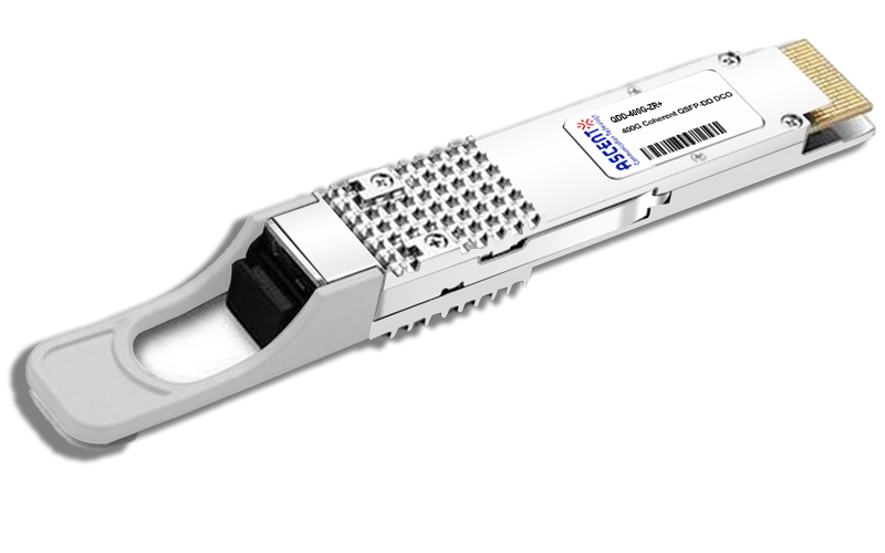

Ascent’s 400G ZR QSFP-DD Digital Coherent Optic Modules are 400 Gb/s Quad Small Form Factor Pluggable-double density (QSFP-DD) transceivers designed for 80 km optical communication applications over a standard pair of G.652 Single-Mode Fiber (SMF).
· Support Flex-grid channel spacing DWDM in C-band
· Support Line-side and Client-side Interfaces:
Line-side: 400G DP-16QAM, Client-side: 400GAUI-8/2*200GAUI-4/4*100GAUI-2
Line-side: 300G DP-8QAM, Client-side: 3*100GAUI-2
Line-side: 200G DP-QPSK, Client-side: 200GAUI-4//2*100GAUI-2/2*CAUI-4 Line-side: 100G DP-QPSK,
Client-side: 100GAUI-2/CAUI-4
· Standard QSFP-DD Type 2 form factor
· 76pin QSFP-DD MSA compliant connector
· Compliant to CMIS 5.0
· Compliant to OIF Implementation Agreement for Coherent CMIS, Rev 01.1
· OpenZR+ Specifications, version 2.0, 29 July 2022
· RoHS compliant
Parameter | Min. | Max. | Unit | Note |
Storage Temperature | -40 | 85 | °C | |
Storage Humidity (Relative) | - | 85 | % | no-condensing |
Case Temperature | 0 | 75 | °C | |
Operating Humidity (Relative) | - | 85 | % | no-condensing |
Short term Operating Case Temperature | 80 | °C | <24 hours | |
Power Supply Absolute Range | -0.3 | 3.63 | V | |
RX Optical Max.imum Input Power | - | 10 | dBm |
Operating Conditions
Parameter Operating Case Temperature | Min. 0 | Max. 75 | Unit °C | Note |
Operating Humidity (Relative) | - | 85 | % | no-Condensing |
Power Supply Operating Range | 3.135 | 3.465 | V | |
RX Optical Input Power | - | 0 | dBm |
Power Supply
The 400G ZR QSFP-DD DCO is a Power Class 8 module. In order to avoid exceeding the host system power capacity, upon hot-plug, power cycle or reset, all QSFP-DD modules shall power up in Low Power Mode if LPMode is asserted. If LPMode is not asserted the module will proceed to High Power Mode without host intervention. Specification values for maximum instantaneous, sustained and steady state currents at each power class are given in below table. The power supply requirements are specified in the table below.
Parameter | Min. | Typ. | Max. | Unit | Note |
3.3V DC Power Supply Voltage | 3.135 | 3.3 | 3.465 | V | |
3.3V DC Power Supply Current | 8 | A | |||
Power Dissipation | 23 | W | 400G | ||
23 | W | 300G | |||
22 | W | 200G | |||
16 | W | 100G | |||
Low Power Consumption | 1.5 | W | |||
Module Inrush Current | 100 | mA/us | |||
Turn-off Current | -100 | mA/us | |||
Power Supply Noise | 25 | mV |
Parameter | Min. Typ. | Max. | Unit | Note |
CEI-56G-VSR-PAM4 | ||||
Signal Rate, each Lane | 26.5625±100ppm | GBaud | ||
Differential Peak-Peak Input Voltage Tolerance | 900 | mVpp | ||
CEI-28G-VSR | ||||
Signal Rate, each Lane | 25.78125±100ppm | |||
Differential Peak-Peak Input Voltage Tolerance | 900 | mVpp |
Electrical Characteristics for Receiver
Parameter | Min. | Typ. | Max. | Unit Note |
CEI-56G-VSR-PAM4 | ||||
Signal Rate, each Lane | 26.5625±100ppm | GBaud | ||
Differential Peak-Peak Input Voltage Tolerance | 900 | mVpp | ||
Transition Time, 20% to 80% | 9 | 9.5 | ps | |
CEI-28G-VSR | ||||
Signal Rate, each Lane | 25.78125±100ppm | |||
Differential Peak-Peak Input Voltage Tolerance | 900 | mVpp | ||
Transition Time, 20% to 80% | 9 | 9.5 | ps | |
Optical Specifications
All specifications given in this document are End-of-Life numbers and are valid under operating conditions unless specific noted:
Optical Transmitter Specifications
Parameter | Min. | Typ. | Max. | Unit | Notes |
Transmitter Frequency Range | 191.3 | 193.7 | 196.1 | THz | 1 |
Laser Frequency Stability | -1.8 | 1.8 | GHz | Frequency stability relative to ITU grid. | |
Laser Frequency Accuracy | -1.8 | 1.8 | GHz | ||
Laser Frequency Fine Tuning Range | -6.0 | 6.0 | GHz | ||
Fine Tuning Resolution | 100 | MHz | |||
Channel Tuning Speed | - | 60 | s | ||
Laser LineWidth | 100 | kHz | |||
Transmitter Output Power Range | -10 | -6 | dBm | 400G OpenZR+ | |
-10 | -6 | dBm | 300G | ||
-9 | -5 | dBm | 200G | ||
-8 | -4 | dBm | 100G | ||
Transmitter Output Disable Time | 180 | ms | |||
Output Power Stability | -0.5 | 0.5 | dB | 2 | |
Output Power Accuracy | -2 | 2 | dB | 3 | |
Transmitter Turn-up Time from Cold Start | - | 120 | s | ||
Transmitter OSNR (Inband) | 34 | - | dB/0.1 nm | ||
Transmitter Back Reflectance | - | -24 | dB | ||
Transmitter Output Power with TX Disabled | - | -20 | dBm | ||
Transmitter Polarization Dependent Power | - | 1.5 | dB | Power deference between X and Y polarization |
1. C band 75GHz ITU-T grid. Frequency range over which the specifications hold unless noted otherwise.
2. Difference over temperature, time, wavelength and aging.
3. Difference between the set value and actual value over aging.
Optical Receiver Specifications
Parameter | Min. | Typ. | Max. | Unit | Notes | |
Receiver Frequency Range | 191.3 | 193.7 | 196.1 | THz | ||
Input Power Range | -12 | 0 | dBm | 1 | ||
-15 | 0 | 2 | ||||
-18 | 0 | 3 | ||||
-18 | 0 | 4 | ||||
OSNR Sensitivity | 22 | 24 | dB/0.1 nm | 400G | ||
21 | 300G | |||||
16 | 200G | |||||
12.5 | 100G | |||||
Receiver Sensitivity | -22 | dBm | 400G | |||
-26 | 300G | |||||
-30 | 200G | |||||
-34 | 100G | |||||
CD Tolerance | 20000 | ps/nm | 5 | |||
40000 | 6 | |||||
50000 | 7 | |||||
100000 | 8 | |||||
PMD (avg) Tolerance | 20 | ps | 5 | |||
25 | 6 | |||||
25 | 7 | |||||
30 | 8 | |||||
Peak PDL Tolerance | 3.0 | dB | 9 | |||
3.5 | dB | 10 | ||||
Tolerance to Change in SOP | 50 | - | rad/ms | 11 | ||
Input Power Transient Tolerance | -2 | 2 | dB | 12 | ||
Input Power Reading Accuracy | -2 | 2 | dB | |||
Optical Return Loss | 20 | dB | Optical reflectance at Rx connector input. | |||
Receiver Turn-up Time from Cold Start | 120 | s | 13 | |||
1. Signal power of the channel at the OSNR Penalty < 0.5dB for 400G
2. Signal power of the channel at the OSNR Penalty < 0.5dB for 300G
3. Signal power of the channel at the OSNR Penalty < 0.5dB for 200G
4. Signal power of the channel at the OSNR Penalty < 0.5dB for 100G
5. Tolerance to CD with ≤0.5 dB penalty to OSNR sensitivity when change in SOP is ≤1 rad/ms for 400G.
6. Tolerance to CD with ≤0.5 dB penalty to OSNR sensitivity when change in SOP is ≤1 rad/ms for 300G.
7. Tolerance to CD with ≤0.5 dB penalty to OSNR sensitivity when change in SOP is ≤1 rad/ms for 200G.
8. Tolerance to CD with ≤0.5 dB penalty to OSNR sensitivity when change in SOP is ≤1 rad/ms for 100G.
9. Tolerance to peak PDL with ≤1.3 dB additional OSNR penalty when change in SOP is ≤1 rad/ms.
10. Tolerance to peak PDL with ≤1.8 dB additional OSNR penalty when change in SOP is ≤1 rad/ms.
11. With ≤0.5 dB additional OSNR penalty over all PMD and PDL values.
12. Tolerance to change in input power with<0.5 dB penalty to OSNR sensitivity.
13. From module reset, with valid optical input signal present.
Loopback
The module support loopback functionality. The host loopback (Loopback ①) and the network loopback (Loopback ②) are shown at bellowing figure. For details on controlling the loopback mode, please refer to Reference [2]. In optional loopback, TXn is looped back to RXn, for example TX0+ to RX0+, on both host and media side.
Insertion, Extraction and Retention Force
The following table details the mechanical forces to insert, remove, and retain the module in a standard QSFP-DD card cage.
Parameter | Min. | Max. | Unit Note |
Insertion Force | 90 | N | |
Extraction Force | 50 | N | |
Retention Force | 90 | N |
EMI, EMC and ESD Specifications
The module is compliant with the requirements listed in the table below when installed in the host equipment.
Parameter | Reference | Value | Unit | Note |
ESD Immunity | IEC 61000-4-2 | 8 | kV | Contact Discharge |
15 | kV | Air Discharge | ||
ESD (HBM model) | JEDEC JESD22-A114-B | 1 | kV | High-Speed Contacts |
2 | kV | Other pins | ||
EMC Immunity | IEC 61000-4-3 | |||
EMI Emission | FCC Class B |
Laser Safety
This is a Class 1 Laser Product according to IEC 60825-1:2007. This product complies with 21 CFR 1040.10 and 1040.11 except for deviations pursuant to Laser Notice No. 50, dated (June 24, 2007).Don’t directly look into the transmitter fiber connector at any time while the module is in operation.

The key application for the ZR standard is allowing the transmission of a 400G wavelength in point-to-point topology to a distance of 120 km or longer with the Mux/Demux and Amplifier as depicted the below.
Ascent A1600 1U, 2U and 4U DCI platforms are highly integrated, compact in size. It features standard 19” 1U, 2U, 4U chassis, power supply (AC/DC optional), 1+1 backup, ready to install. 1U, 2U, and 4U transmission platforms support max 4, 8 and 16 services slots, mixed different interface modules (hot pluggable) such as Mux/Demux, Amplifiers, and in-band and out-of-band network management, flexible bandwidth per channel, remote update, easy maintenance.
800G OSFP DAC Cable
800G OSFP ACC Cable
800G OSFP DR8 1310 nm 500 m
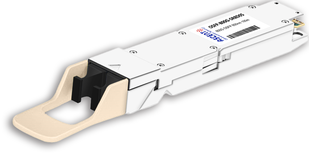
800G OSFP SR8 850 nm 100 m
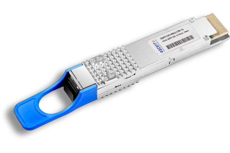
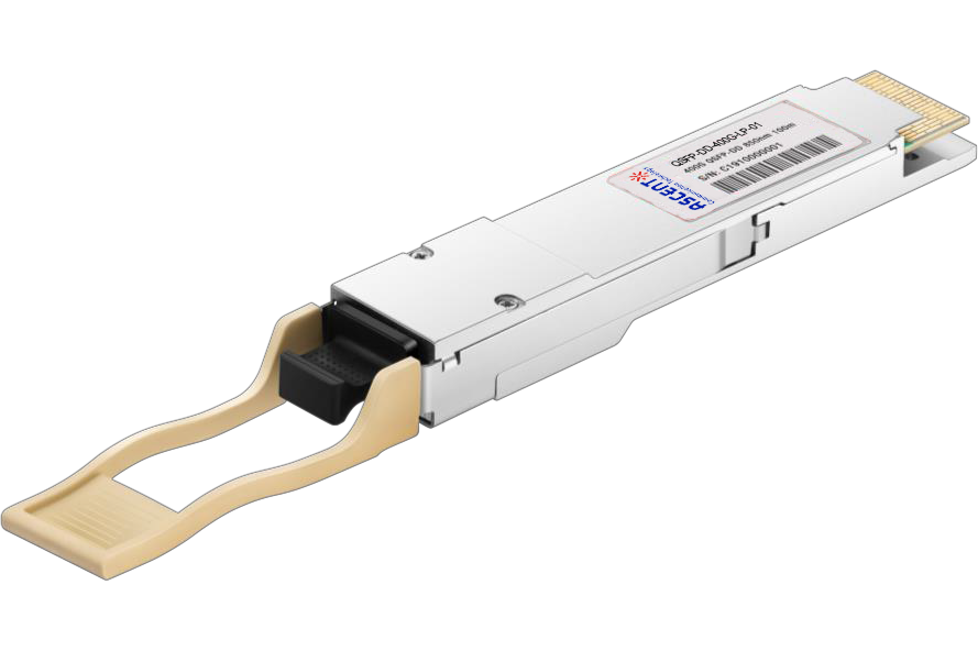
400G QSFP56-DD 10km
400G QSFP-DD ER8 40 km
400G QSFP-DD LR8 1310 nm 10 km

400G QSFP-DD LR4 CWDM 10 km
400G QSFP-DD SR8 850 nm 100 m
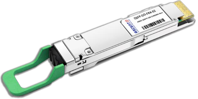
400G QSFP-DD FR4 2km
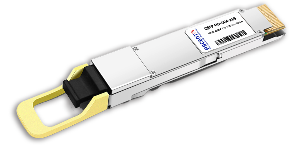
400G QSFP-DD DR4 500m
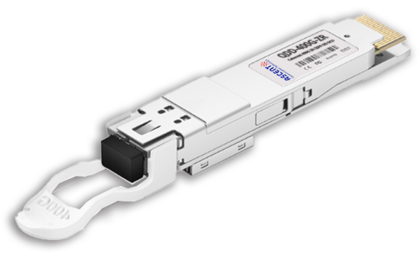
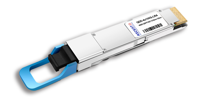
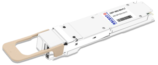
400G QSFP-DD DCO ZR
4X100G QSFP-DD LR4 10km
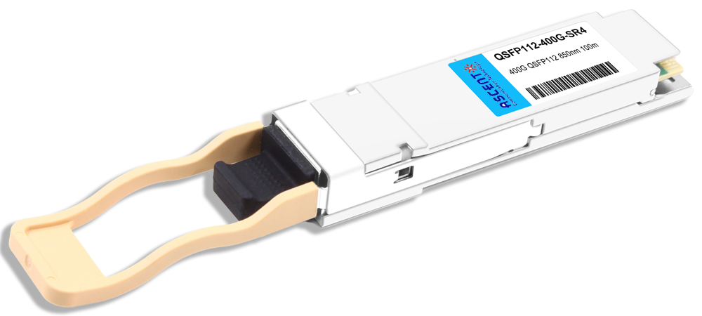
400G QSFP112 SR4 850 nm 100 m

400G QSFP112 DR4 1310 nm 500 m
400G OSFP SR4 FLT 50m Transceiver
400G OSFP SR8 100m Transceiver