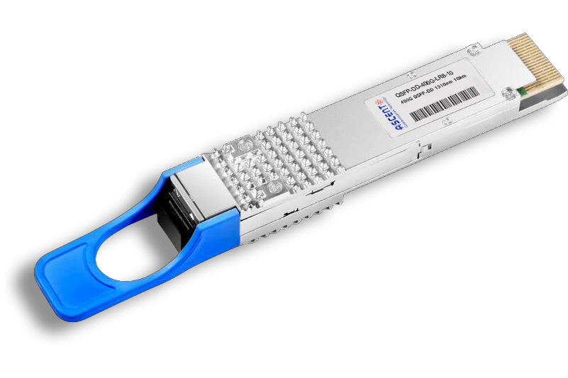
Ascent’s QSFP-DD-LR4-10 is a 400Gb/s Quad Small Form Factor Pluggable-double density (QSFP-DD) optical module designed for 10km optical communication applications. The module converts 8 channels of 50Gb/s (PAM4) electrical input data to 4 channels of CWDM optical signals, and multiplexes them into a single channel for 400Gb/s optical transmission. Reversely, on the receiver side, the module optically de-multiplexes a 400Gb/s optical input into 4 channels of CWDM optical signals, and converts them to 8 channels of 50Gb/s (PAM4) electrical output data. The central wavelengths of the 4 CWDM channels are 1271, 1291, 1311 and 1331 nm as members of the CWDM wavelength grid defined in ITU-T G.694.2. It contains a duplex LC connector for the optical interface and a 76-pin connector for the electrical interface. To minimize the optical dispersion in the long-haul system, single-mode fiber (SMF) has to be applied in this module. Host FEC is required to support up to 10km fiber transmission The product is designed with form factor, optical/electrical connection and digital diagnostic interface according to the QSFP-DD Multi-Source Agreement (MSA) Type 2. It has been designed to meet the harshest external operating conditions including temperature, humidity and EMI interference.
· QSFP-DD MSA compliant
· 4 CWDM lanes MUX/DEMUX design
· 100G Lambda MSA 400G-LR Specification compliant
· Up to 10km transmission on single mode fiber (SMF) with FEC
· Operating case temperature: 0 to 70℃
· 8x53.125Gb/s electrical interface (400GAUI-8)
· Data Rate 106.25Gbps (PAM4) per channel.
· Maximum power consumption 12W
· Duplex LC connector
· RoHS compliant
Absolute Maximum Ratings
It has to be noted that the operation in excess of any individual absolute maximum ratings might cause permanent damage to this module.
Parameter | Symbol | Min. | Typ. | Max. | Unit | Note |
Storage Temperature | TS | -40 | 85 | °C | ||
Operating Case Temperature | TOP | 0 | 70 | °C | ||
Power Supply Voltage | VCC | -0.5 | 3.6 | V | ||
Relative Humidity (non-condensation) | RH | 0 | 85 | % | ||
Parameter | Symbol | Min. | Typ. | Max. | Unit | Note |
Operating Case Temperature | TOP | 0 | 70 | °C | ||
Power Supply Voltage | VCC | 3.135 | 3.3 | 3.465 | V | |
Data Rate, each Lane | 26.5625 | GBd | PAM4 | |||
Data Rate Accuracy | -100 | 100 | ppm | |||
Pre-FEC Bit Error Ratio | 2.4x10⁻⁴ | |||||
Post-FEC Bit Error Ratio | 1x10-12 | 1 | ||||
Link Distance | D | 0.5 | 10 | km | 2 |
Notes:
1. FEC provided by host system.
2. FEC required on host system to support maximum distance.
Optical Characteristics
Parameter | Symbol | Min. | Typ. | Max. | Unit | Note |
Wavelength Assignment | L0 | 1264.5 | 1271 | 1277.5 | nm | |
L1 | 1284.5 | 1291 | 1297.5 | nm | ||
L2 | 1304.5 | 1311 | 1317.5 | nm | ||
L3 | 1324.5 | 1331 | 1337.5 | nm | ||
Transmitter | ||||||
Data Rate, each Lane | 53.125 ± 100 ppm | GBd | ||||
Modulation Format | PAM4 | |||||
Side-mode Suppression Ratio | SMSR | 30 | dB | Modulated | ||
Total Average Launch Power | PT | 10 | dBm | |||
Average Launch Power, each Lane | PAVG | -1.4 | 4.5 | dBm | 1 | |
Outer Optical Modulation Amplitude (OMAouter), each Lane | POMA | 0.7 | 4.7 | dBm | 2 | |
Launch Power in OMAouter Minus TDECQ, each Lane | -0.7 | dB | For ER ≥4.5dB | |||
Launch Power in OMAouter Minus TDECQ, each Lane | -0.6 | dB | For ER<4.5dB | |||
Transmitter and Dispersion Eye Clouser for PAM4, each Lane | TDECQ | 3.4 | dB | |||
Extinction Ratio | ER | 3.5 | dB | |||
Difference in Launch Power between any Two Lanes(OMAouter) | 4 | dB | ||||
RIN15.6OMA | RIN | -136 | dB/Hz | |||
Optical Return Loss Tolerance | TOL | 17.1 | dB | |||
Transmitter Reflectance | TR | -26 | dB | |||
Transmitter Transition Time | 17 | ps | ||||
Average Launch Power of OFF Transmitter, each Lane | Poff | -20 | dBm | |||
Receiver | ||||||
Data Rate, each Lane | 53.125 ± 100 ppm | GBd | ||||
Modulation Format | PAM4 | |||||
Damage Threshold, each Lane | THd | 5.5 | dBm | 3 | ||
Average Receive Power, each Lane | -7.7 | 4.5 | dBm | 4 | ||
Receive Power (OMAouter), each Lane | 4.7 | dBm | ||||
Difference in Receiver Power between any Two Lanes(OMAouter) | 4.1 | dB | ||||
Receiver Sensitivity (OMAouter), each Lane | SEN | -6.6 | dBm | For BER of 2.4E-4 | ||
Stressed Receiver Sensitivity (OMAouter), each Lane | SRS | See below picture | dBm | 5 | ||
Receiver Reflectance | RR | -26 | dB | |||
LOS Assert | LOSA | -30 | dBm | |||
LOS De-assert | LOSD | -12 | dBm | |||
LOS Hysteresis | LOSH | 0.5 | dB | |||
Stressed Conditions for Stress Receiver Sensitivity (Note 6) | ||||||
Stressed Eye Closure for PAM4 (SECQ), Lane under Test | 0.9 | 3.4 | dB | |||
OMAouter of each Aggressor Lane | 1.5 | dBm | ||||
Notes:
1. Average launch power, each lane (min) is informative and not the principal indicator of signal strength. A transmitter with launch power below this value cannot be compliant; however, a value above this does not ensure compliance.
2. Even if the TDECQ < 1.4 dB for an extinction ratio of ≥ 4.5 dB or TDECQ < 1.3 dB for an extinction ratio of < 4.5 dB, the OMAouter (min) must exceed the minimum value specified here.
3. The receiver shall be able to tolerate, without damage, continuous exposure to an optical input signal having this average power level.
4. Average receive power, each lane (min) is informative and not the principal indicator of signal strength. A received power below this value cannot be compliant; however, a value above this does not ensure compliance.
5. Measured with conformance test signal for BER = 2.4x10⁻⁴. A compliant receiver shall have stressed receiver sensitivity (OMAouter), each lane values below the mask of Figure 4, for SECQ values between 0.9 and 3.4 dB.
6. These test conditions are for measuring stressed receiver sensitivity. They are not characteristics of the receiver.

Electrical Characteristics
The following electrical characteristics are defined over the Recommended Operating Environment unless otherwise specified.
Parameter | Symbol | Min. | Typ. | Max. | Unit | Note |
Power Consumption | 12 | W | ||||
Supply Current | Icc | 3.64 | A | |||
Transmitter (each Lane) | ||||||
Signaling Rate, each Lane | TP1 | 26.5625 ± 100 ppm | GBd | |||
Differential pk-pk Input Voltage Tolerance | TP1a | 900 | mVpp | 1 | ||
Differential Termination Mismatch | TP1 | 10 | % | |||
Differential Input Return Loss | TP1 | IEEE 802.3-2015 Equation (83E-5) | dB | |||
Differential to Common Mode Input Return Loss | TP1 | IEEE 802.3-2015 Equation (83E-6) | dB | |||
Module Stressed Input Test | TP1a | See IEEE 802.3bs 120E.3.4.1 | 2 | |||
Single-ended Voltage Tolerance Range (Min) | TP1a | -0.4 to 3.3 | V | |||
DC Common Mode Input Voltage | TP1 | -350 | 2850 | mV | 3 | |
Receiver (each Lane) | ||||||
Signaling Rate, each lane | TP4 | 26.5625 ± 100 ppm | GBd | |||
Differential Peak-to-Peak Output Voltage | TP4 | 900 | mVpp | |||
AC Common Mode Output Voltage, RMS | TP4 | 17.5 | mV | |||
Differential Termination Mismatch | TP4 | 10 | % | |||
Differential Output Return Loss | TP4 | IEEE 802.3-2015 Equation (83E-2) | ||||
Common to Differential Mode Conversion Return Loss | TP4 | IEEE 802.3-2015 Equation (83E-3) | ||||
Transition Time, 20% to 80% | TP4 | 9.5 | ps | |||
Near-end Eye Symmetry Mask Width (ESMW) | TP4 | 0.265 | UI | |||
Near-end Eye Height, Differential | TP4 | 70 | mV | |||
Far-end Eye Symmetry Mask Width (ESMW) | TP4 | 0.2 | UI | |||
Far-end Eye Height, Differential | TP4 | 30 | mV | |||
Far-end Pre-cursor ISI Ratio | TP4 | -4.5 | 2.5 | % | ||
Common Mode Output Voltage (Vcm) | TP4 | -350 | 2850 | mV | 3 | |
Notes:
1. With the exception to IEEE 802.3bs 120E.3.1.2 that the pattern is PRBS31Q or scrambled idle.
2. Meets BER specified in IEEE 802.3bs 120E.1.1.
3. DC common mode voltage generated by the host. Specification includes effects of ground offset voltage.
Digital Diagnostics
Parameter | Range | Min | Max | Units | Notes |
Temperature Monitor Absolute Error | DMI_Temp | -3 | 3 | degC | Over operating temperature range |
Supply Voltage Monitor Absolute Error | DMI _VCC | -0.1 | 0.1 | V | Over full operating range |
Channel RX Power Monitor Absolute Error | DMI_RX_Ch | -2 | 2 | dB | 1 |
Channel Bias Current Monitor | DMI_Ibias_Ch | -10% | 10% | mA | |
Channel TX Power Monitor Absolute Error | DMI_TX_Ch | -2 | 2 | dB | 1 |
Notes:
1. Due to measurement accuracy of different single mode fibers, there could be an additional +/-1 dB fluctuation, or a +/- 3 dB total accuracy.
ESD
This transceiver is specified as ESD threshold 1kV for high speed data pins and 2kV for all other electrical input pins, tested per MIL-STD-883, Method 3015.4 /JESD22-A114-A (HBM). However, normal ESD precautions are still required during the handling of this module. This transceiver is shipped in ESD protective packaging. It should be removed from the packaging and handled only in an ESD protected environment.
Laser Safety
This is a Class 1 Laser Product according to EN 60825-1:2014. This product complies with 21 CFR 1040.10 and 1040.11 except for deviations pursuant to Laser Notice No. 50, dated (June 24, 2007).
Caution: Use of controls or adjustments or performance of procedures other than those specified herein may result in hazardous radiation exposure.


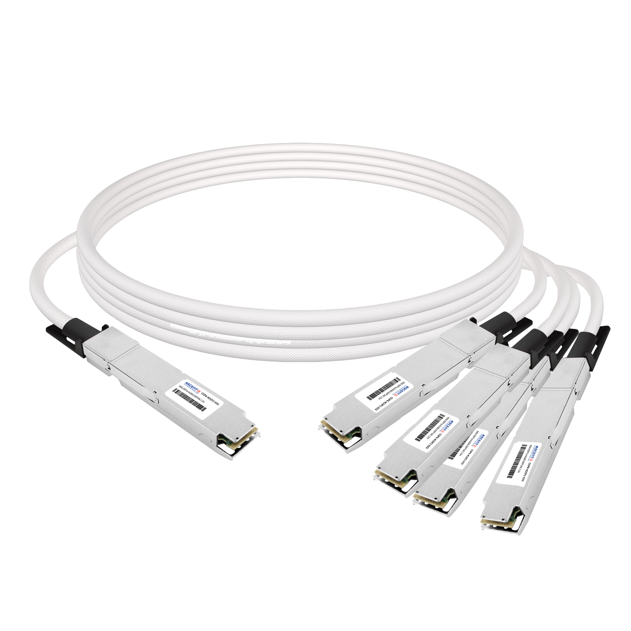
800G OSFP DAC Cable
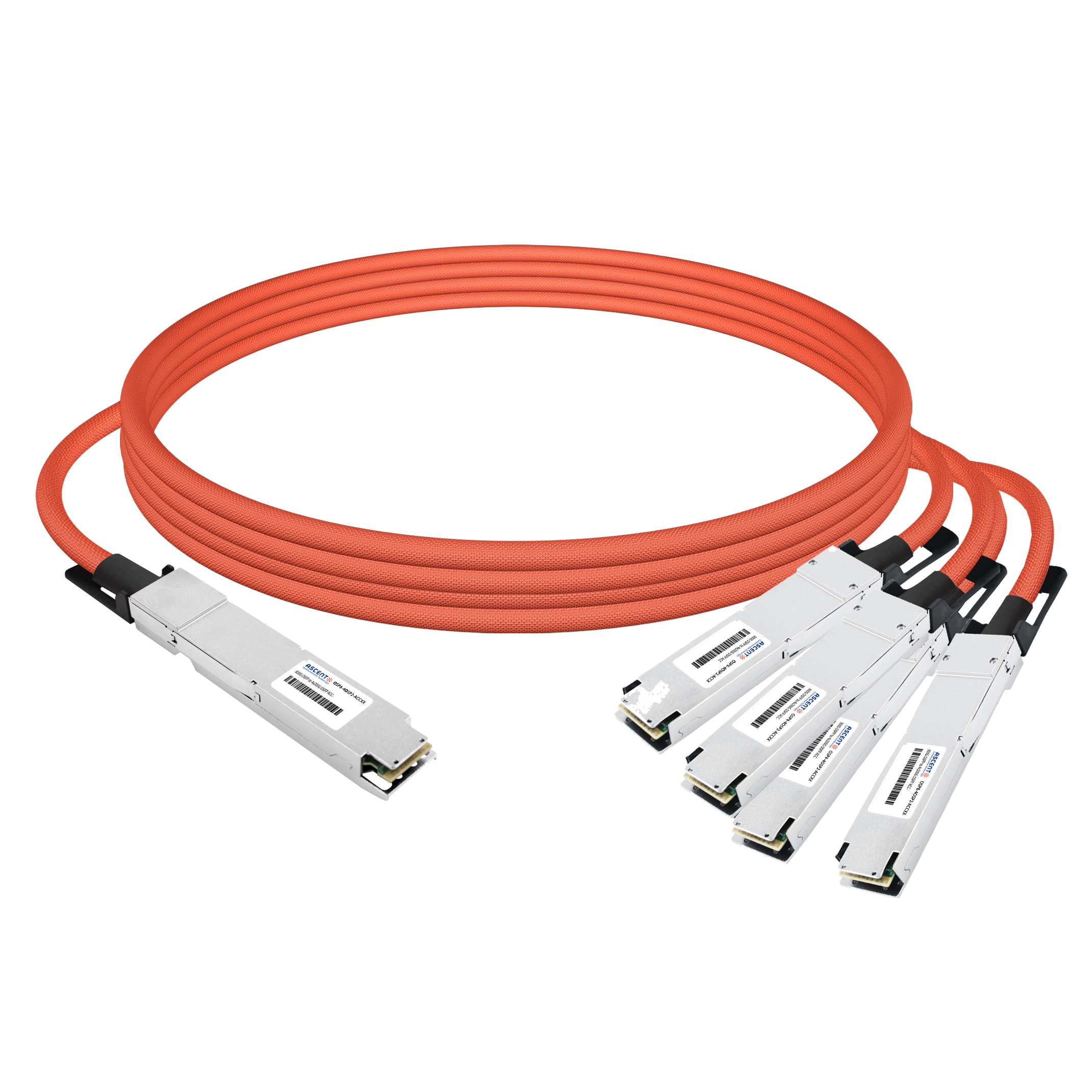
800G OSFP ACC Cable
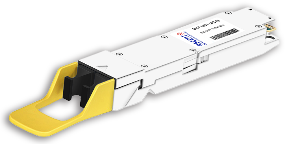
800G OSFP DR8 1310 nm 500 m
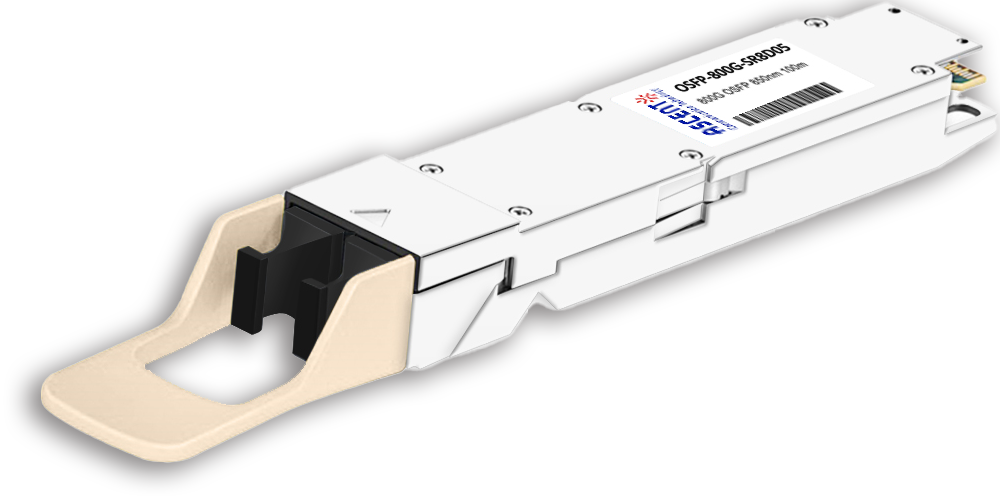
800G OSFP SR8 850 nm 100 m
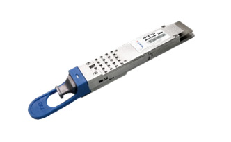
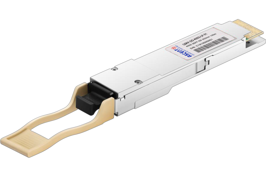
400G QSFP56-DD 10km
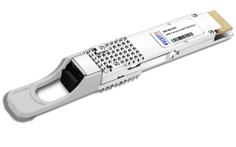
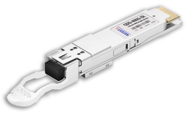
400G QSFP-DD ZR+
400G QSFP-DD ER8 40 km
400G QSFP-DD LR8 1310 nm 10 km
400G QSFP-DD SR8 850 nm 100 m
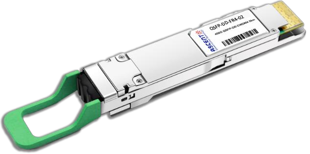
400G QSFP-DD FR4 2km
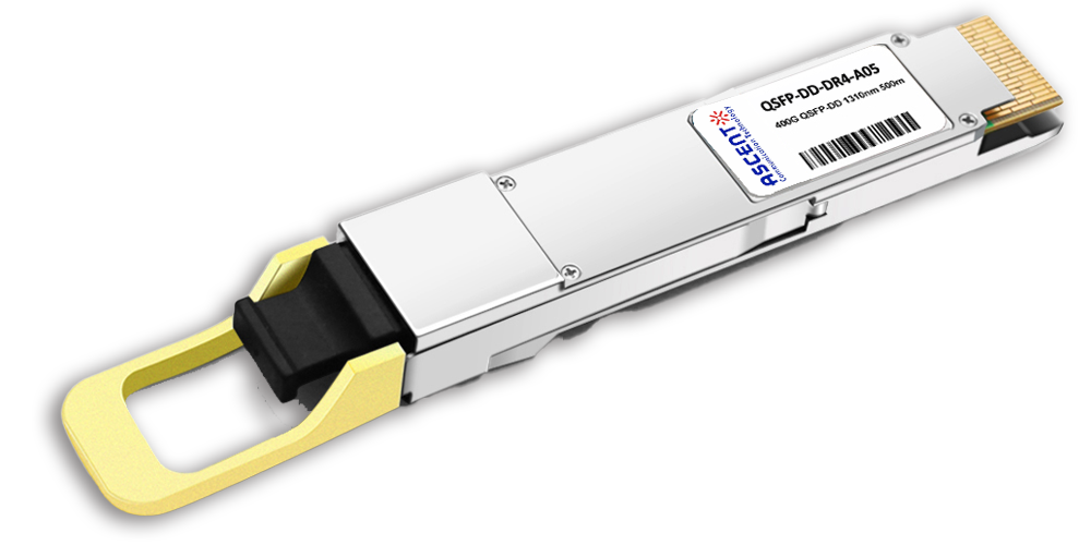
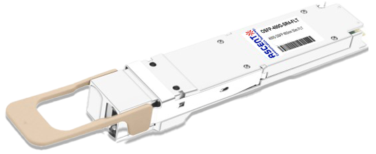
400G QSFP-DD DR4 500m
400G QSFP-DD DCO ZR
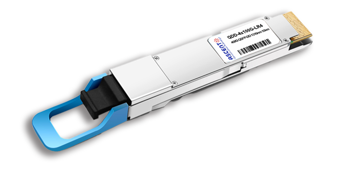
4X100G QSFP-DD LR4 10km
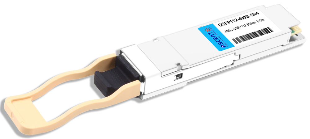
400G QSFP112 SR4 850 nm 100 m
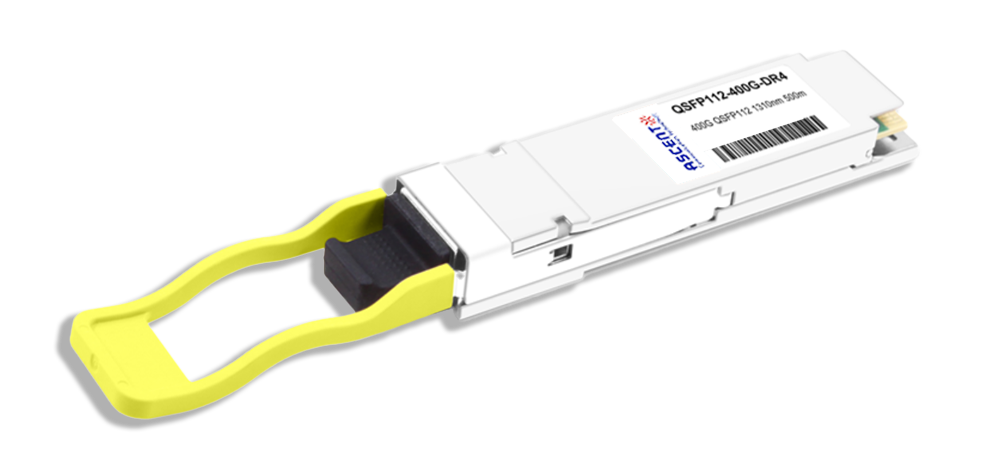
400G QSFP112 DR4 1310 nm 500 m
400G OSFP SR4 FLT 50m Transceiver
400G OSFP SR8 100m Transceiver