Ascent’s QSFP-AQ-MP-31-02 optical transceiver is intended for up to 2km reach service with four-lane 10.3125G data rate. It is based on 3.3V DC power supply and operates in the commercial temperature range. It is compliant with QSFP MSA, SFF-8436 and IEEE802.3ba-2018. Digital diagnostic functions are available via I2C interface, and the control functions can be achieved by LVTTL interfaces on the host, mainly including Module Select (ModSelL), Module Reset (ResetL), Low Power Mode (LPMode). The transceiver incorporates a four-laser array which is usually DFB, four-PIN diode array, an integrated four drivers and TIAs IC separately. The differential AC coupled Tx and Rx data interfaces are CML compatible.
· MPO-12 optical interface
· Maximum link length up to 2km
· Up to 10.3125Gb/s data links per lane
· +3.3 V power supply
· QSFP MSA compliant package
· Hot Pluggable
· High performance singal mode DML transmitter
· High sensitivity PIN/TIA optical receiver
· Single Mode operation
· BER < 1E-12@-13.6dBm (OMA)
· Case Operating temperature : 0 to 70 °C
· Data and Control Interfaces
· Tx Data CML/AC Coupled
· Rx Data CML/AC Coupled
· ModSelL LVTTL
· ResetL LVTTL
· ModPrsL LVTTL
· LPMode LVTTL
· 2-wire I2C communication bus
· RoHS 6 compliance
Parameter | Symbol | Min. | Max. | Units | Notes |
Storage Temperature | Tstg | -40 | +95 | °C | |
Case Operating Temperature | TO | 0 | +70 | °C | |
Relative Humidity - Storage | RHS | 0 | 95 | % | |
Relative Humidity - Operating | RHO | 0 | 85 | % | |
Supply Voltage | VCC | -0.3 | 3.6 | V |
Parameter | Symbol | Min. | Typ. | Max. | Unit | Notes |
Case Operating Temperature | Tcase | 0 | - | +70 | °C | |
DC Supply Voltage | VCC | 3.135 | - | 3.465 | V | |
Module Supply Current | Iin | - | - | 1060 | mA |
Parameter | Symbol | Min. | Typ. | Max. | Unit | Notes |
Transmitter | ||||||
Signaling Speed per Lane | 10.3125±100ppm | Gbps | ||||
Lane Wavelength | L0 | 1295 | 1310 | 1325 | nm | |
L1 | 1295 | 1310 | 1325 | nm | ||
L2 | 1295 | 1310 | 1325 | nm | ||
L3 | 1295 | 1310 | 1325 | nm | ||
Side Mode Suppression Ratio | SMSR | 30 | dB | |||
Average Launch Power|Each Lane | Pavg | -7 | 2.5 | dBm | ||
Optical Modulation Amplitude|Each Lane | OMA | 2.5 | dBm | 1 | ||
Transmitter and Dispersion Penalty|Each Lane | TDP | 2.6 | dB | |||
Eye Mask coordinates: X1, X2, X3, Y1, Y2, Y3 | {0.25, 0.4, 0.45, 0.25, 0.28, 0.4} | dBm | ||||
Average Launch Power of OFF Transmitter|Each Lane | -30 | dBm | ||||
Extinction Ratio | ER | 3.5 | dB | |||
Spectral Width|20dB | 1 | nm | ||||
Transmitter Reflectance | -12 | dB | ||||
Optical Return Loss Tolerance | 20 | dB | ||||
Receiver | ||||||
Signal Speed Per Lane | 10.3125±100ppm | Gbps | ||||
Lane Wavelength | L0 | 1295 | 1310 | 1325 | nm | |
Center Wavelength Lane 1 | L1 | 1295 | 1310 | 1325 | nm | |
Center Wavelength Lane 2 | L2 | 1295 | 1310 | 1325 | nm | |
Center Wavelength Lane 3 | L3 | 1295 | 1310 | 1325 | nm | |
Damage Threshold|Each Lane | THd | 2.5 | dBm | 2 | ||
Average Receive Power|Each Lane | -11.6 | 2 | dBm | |||
Receiver Reflectance | -26 | dB | ||||
Sensitivity OMA|Each Lane [1] | Sen1 | -11 | dBm | 3 | ||
Parameter | Symbol | Min. | Typ. | Max. | Unit | Notes |
Stressed Receiver Sensitivity (OMA), each Lane | -8.6 | dBm | ||||
LOS Assert | LOSA | -30 | - | dBm | ||
LOS Deassert | LOSD | -17 | dBm | |||
LOS Hysteresis | LOSH | 0.5 | 5 | dB | ||
Vertical Eye Closure Penalty | VECP | 1.9 | dB | 4 | ||
Stressed Eye J2 Jitter | J2 | 0.3 | UI | |||
Stressed Eye J4 Jitter | J4 | 0.47 | UI | |||
Notes:
1. Even if the TDP < 0.8dB, the OMA min must exceed the minimum value specified here.
2. The receiver shall be able to tolerate, without damage, continuous exposure to a modulated optical input
signal having this power level on one lane. The receiver does not have to operate correctly at this input power.
3. Measured with conformance test signal at receiver input for BER = 1e-12.
4. Vertical eye closure penalty and stressed eye jitter are test conditions for measuring stressed receiver sensitivity.
5. They are not characteristics of the receiver.
Parameter | Symbol | Min | Typ | Max | Unit | Notes |
Transmitter | ||||||
Differential Data input Swing | Vin | 180 | - | 900 | mV | |
Tx Differential Input Impendence | Zin | 90 | 100 | 110 | Ω | |
Tx Differential Output Impendence | Zout | 45 | 50 | 55 | Ω | |
ResetL Disable Voltage | Vr | 2.0 | - | VCC+0.3 | V | |
ResetL Enable Voltage | VrEN | 0 | - | 0.8 | V | |
ModSelL Disable Voltage | Vm | 2.0 | - | VCC+0.3 | V | |
ModSelL Enable Voltage | VmEN | 0 | - | 0.8 | V | |
Reciever | ||||||
Differential Data Output Swing | Vout | 180 | - | 900 | mV | |
Rx Differential Output Impendence | Zout | 90 | 100 | 110 | Ω | |
IntL Assert Voltage | VInt | VCC-0.5 | - | VCC+0.3 | V | |
IntL De-assert Voltage | VDInt | 0 | - | +0.4 | V | |
Parameter | Symbol | Spec | Units | Condition/Notes |
Temperature | Te | +/-3 | °C | |
Voltage | VCC | +/-5% | V | |
IBias | BIAS | +/-10% | mA | |
Rx power | Rx-pwr | +/-3 | dBm | |
Tx power | Tx-pwr | +/-3 | dBm |


64G SFP56 850nm 100m
40/100G SFP28 SWDM4 100m

40G QSFP+ ER4 Industrial 40 km

40G QSFP+ ER4 40 km

40G QSFP+ LR4 Industrial 10 km

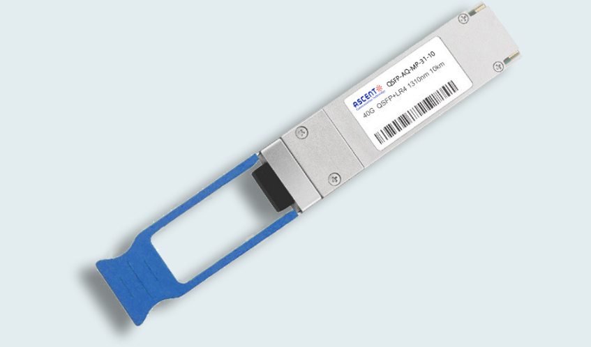
40G QSFP+ LR4 10 km
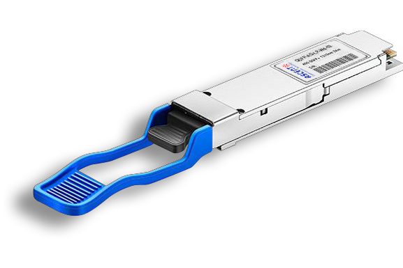
40G QSFP+ PLR4 1310 nm 10 km

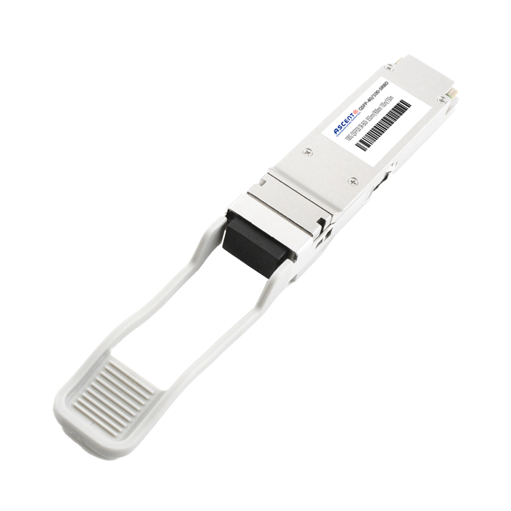
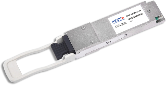
40G QSFP+ CSR4 300m
40GBASE-UNIV QSFP+ MMF and SMF
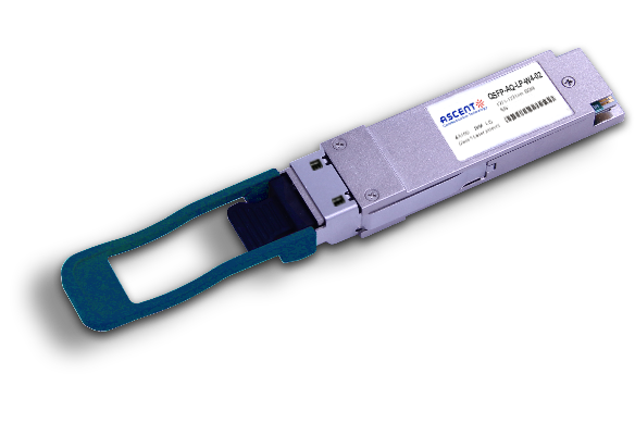
40G QSFP+ CWDM 2 km
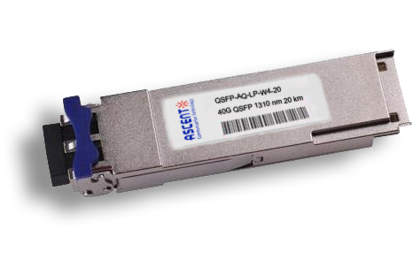
40G QSFP CWDM 20 km
40G QSFP+ SR4 300 m
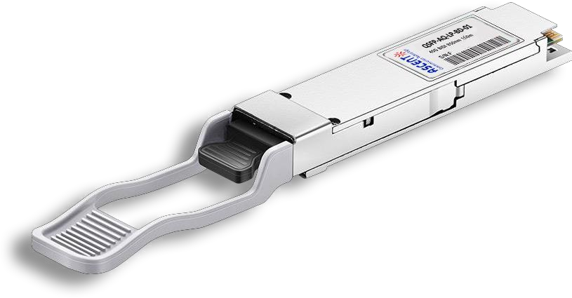
40G QSFP+ BIDI 150m
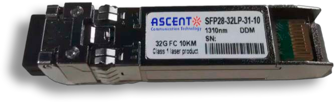
32G SFP28 1310 nm 10 km

32G SFP28 SR 850 nm 100 m
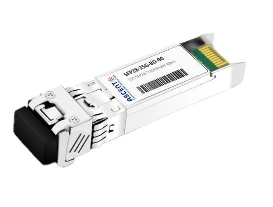
25G SFP28 BIDI 80 km
.png)
25G SFP28 CWDM 10 km(E)
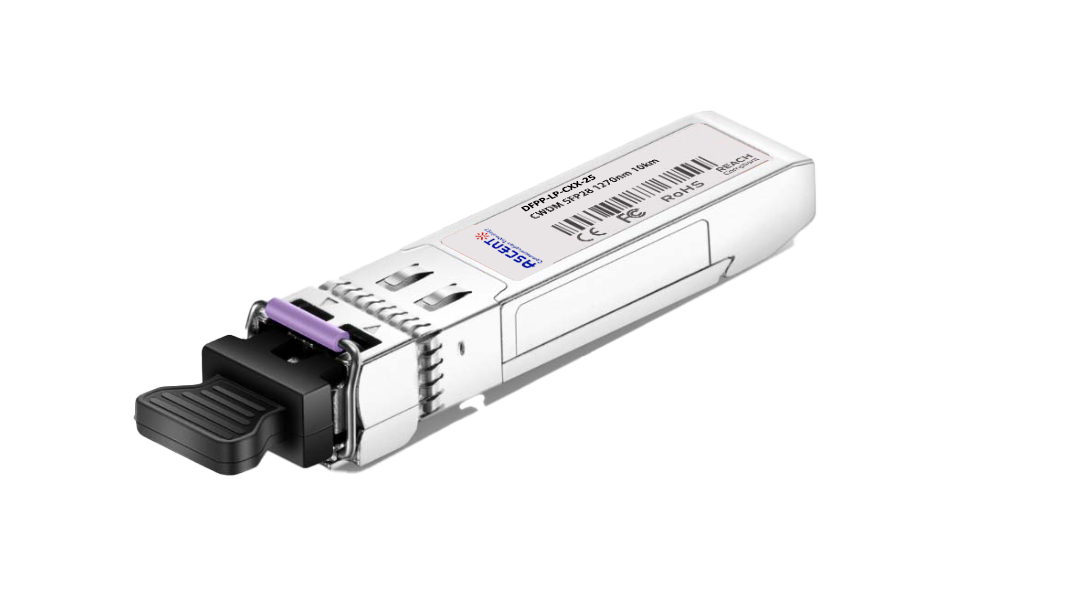
25G SFP28 CWDM 10 km(D)
25G SFP28 ZR 1310nm 80km
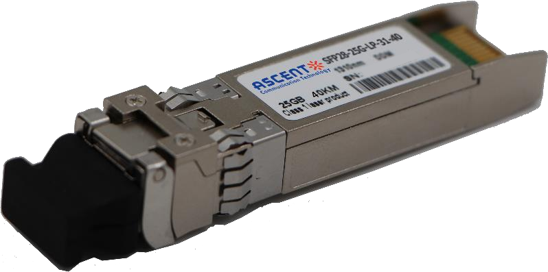
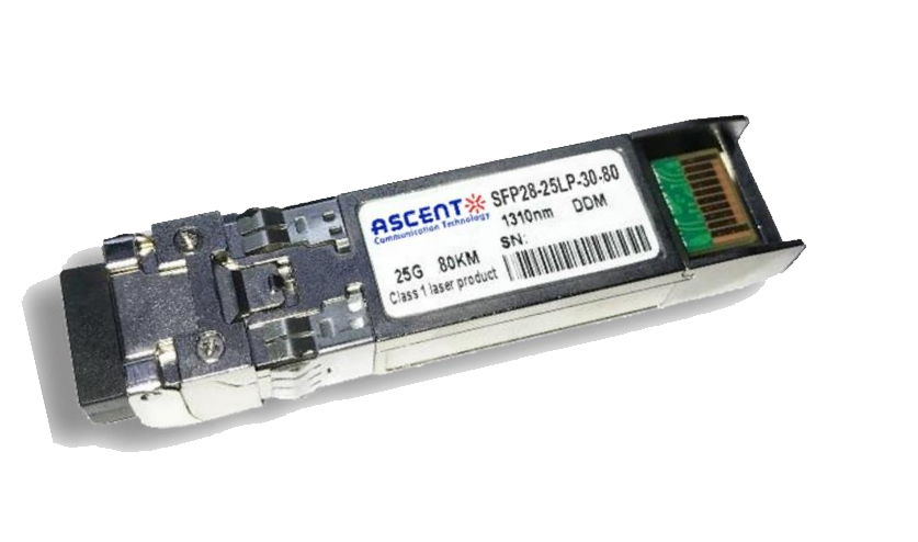
25G SFP28 1310 nm 40km
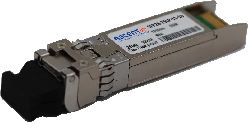
25G SFP28 1310 nm 10 km
25G SFP28 850 nm 300m

10/25G SFP28 1310nm 40km
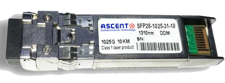
10/25G SFP28 1310nm 10km

10/25G SFP28 850 nm 300m

10/25G SFP28 850 nm 100m