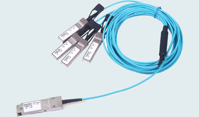
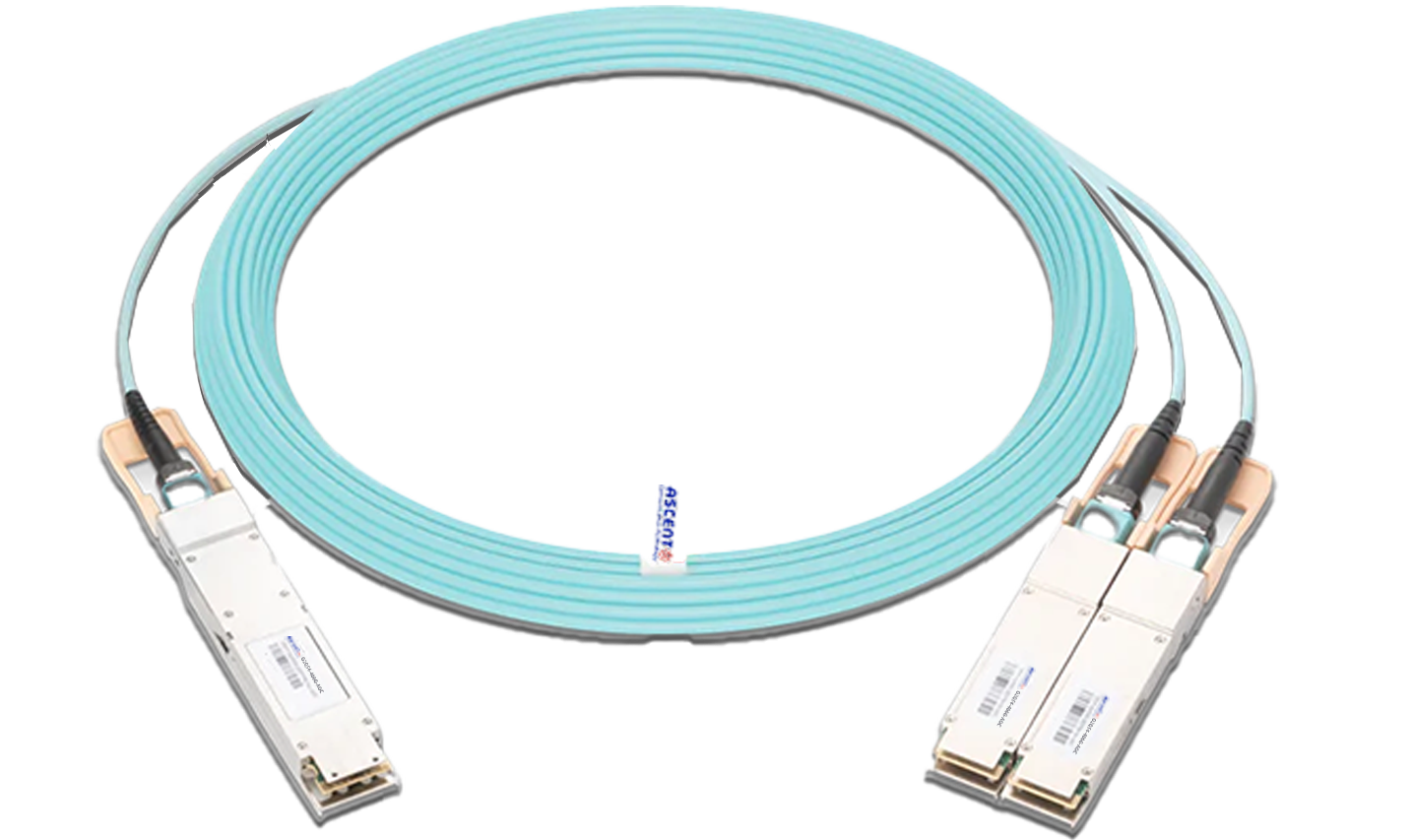
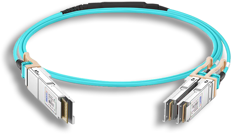
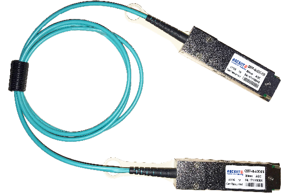
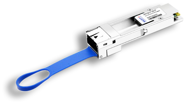
ASCENT 40G QSFP+ to 4x10G SFP+ Active Optical breakout Cable can be used to convert a 40 G QSFP+ input into 4 × 10 G SFP+ outputs for high-speed storage and data applications.
• Supports 40G to 10G Ethernet interoperability
• Aggregate 4 discrete SFP+ 10G channels into single parallel QSFP+ 40G interface
• Maximum link length of 100m links on OM3 multimode fiber Or 150m links on OM4 multimode fiber
• Electrically hot-pluggable
• Electrical interface compliant to QSFP+ connector
• (SFF-8436) and SFP+ connectors (SFF-8431)
• Case operating temperature range:0°C to 70°C
Absolute Maximum Ratings
Parameter | Symbol | Value | Notes |
Storage Temperature | Ts | ‑40 °C to 85 °C | |
Relative Humidity | RH | 5 % to 95 % | |
Power Supply Voltage | Vcc | ‑0.3 V to 4.0 V | |
Signal Input Voltage | Vcc ‑0.3 V to Vcc + 0.3 V |
Recommended Operating Conditions
Parameter | Symbol | Value | Notes |
Case Operating Temperature | Tcase | 0 °C to 70°C | Without air flow |
Power Supply Voltage | Vcc | 3.13 V to 3.46 V, 3.3 V typical | |
Power Supply Current | Icc | 450 mA maximum | Per cable end |
Data Rate | BR | 10.3125 Gbps | Each channel |
General Product Characteristics
Parameter | Value | Notes |
Module Form Factor | QSFP+ | |
Number of Lanes | 4 Tx /Rx | |
Maximum Aggregate Data Rate | 42.0 | |
Maximum Data Rate per Lane | 10.5 | |
Standard Cable Lengths | 3, 5, 7, 10, 50, 100 | 1 |
Protocols Supported | Typical applications include Infiniband, Fiber Channel, 40G Ethernet | |
Electrical Interface and Pin‑out | 38‑pin edge connector | 2 |
Standard Optical Cable Type | Multimode ribbon fiber cable assembly, riser‑rated | |
Maximum Power Consumption per End | 1.5 | |
Management Interface | Serial, I2C‑based, 400 kHz maximum frequency | 3 |
Notes:
1. Please contact sales for other lengths
2. Pin‑out as defined by the QSFP+ MSA
3. As defined by the QSFP+ MSA
Electrical Characteristics
Parameter | Symbol | Value | Notes |
Supply Voltage | Vcc1, VccTx, VccRx | 3.14 V to 3.46 V, 3.3 V typical | |
Supply Current | Icc | 450 mA maximum | |
Transmitter | |||
Differential Data Input Swing | Vin,pp | 180 mV to 1000 mV | 1 |
Single‑Ended Input Voltage tolerance | VinT | ‑0.3 V to 4.0 V | |
Receiver | |||
Vout,pp | 300 to 850 mV | 2 | |
Single‑ended Output Voltage | ‑0.3 V to 4.0 V |
Notes:
1. AC coupled internally. See Figure 1 for input eye mask requirements. Self‑biasing 100Ω differential input.
2. AC coupled with 100Ω differential output impedance. See Figure 2 for output eye mask.

Figure 1 ‑ Transmitter Input Differential Signal Mask

Figure 2 ‑ Receiver Output Differential Signal Mask
High‑Speed Electrical Characteristics per Lane
Parameter‑Inputs | Symbol | Value | Notes |
Reference Differential Input Impedance | Zd | 100 Ω | |
Termination Mismatch | ΔZM | 5% maximum | 1 |
Input AC Common Mode Voltage | 25 mV (RMS) maximum | ||
Differential Input Return Loss | SDD11 | 2, 0.01 GHz to 4.1 GHz | |
SDD11 | 3, 4.1 GHz to 11.1 GHz | ||
Differential to Common Mode Loss | SCD11 | ‑10 dB maximum | 0.01 GHz to 11.1 GHz |
Jitter Tolerance (Total) | TJ | 0.40 UI | |
Jitter Tolerance (Deterministic) | DJ | 0.15 UI |
Notes:
1. See SFF‑8431 section D.15 Termination Mismatch for definition and test recommendations
2. Reflection coefficient given by equation SDD11 (dB) < ‑12 + 2 * SQRT(f), with f in GHz. See Figure 3.
3. Reflection coefficient given by equation SDD11 (dB) < ‑6.3 + 13Log10(f/5.5), with f in GHz. See Figure 3
 Figure 3 ‑ Maximum Transmitter Input and Receiver Output Differential Return Loss
Parameter‑Inputs | Symbol | Value | Notes |
Reference Differential Output Impedance | Zd | 100 Ω | |
Termination Mismatch | ΔZM | 5 % maximum | |
Output AC Common Mode Voltage | 15 mV (RMS) maximum | ||
Differential Output Return Loss | SDD22 | 4, 0.01 GHz to 4.1 GHz | |
SDD22 | 5, 4.1 GHz to 11.1 GHz | ||
Common Mode Output Return Loss | SCC22 | 6, 0.01 GHz to 2.5 GHz | |
SCC22 | ‑3 dB maximum | 2.5 GHz to 11.1 GHz | |
Jitter Tolerance (Total) | TJ | ||
Output Rise and Fall time (20 % to 80 %) | tRH, tFH | 24 ps minimum | |
Deterministic Jitter | DJOUT | 0.38 UI | 7 |
Total Jitter | TJOUT | 0.64 UI | 7 |
Notes:
4. Reflection coefficient given by equation SDD22 (dB) < ‑12 + 2 * SQRT(f), with f in GHz. See Figure 3.
5. Reflection coefficient given by equation SDD22 (dB) < ‑6.3 + 13Log10(f/5.5), with f in GHz. See Figure 3.
6. Reflection coefficient given by equation SCC22 (dB) < ‑7 + 1.6 * f, with f in GHz.
7. When transmitter input jitter specs are met.

OSFP 800G ACC Cable
OSFP 800G DAC Cable
800G OSFP to 4x200G Breakout ACC

400G OSFP to 400G QSFP-DD DAC

400G OSFP to 4x100G QSFP56 DAC
400G OSFP to 2x200G QSFP56 AOC Breakout Cable

400G QSFP DD DAC Cable

400G QSFP DD to 4X100G QSFP56 AOC

400G QSFP DD to 4X100G QSFP28 AOC

400G QSFP DD AOC Cable
400G QSFP DD AOC Breakout Cable

200G QSFP56 InfiniBand HDR AOC

200G QSFP56 PSM4 DAC
QSFP28 100G AOC Cable
QSFP28 100G DAC Cable

QSFP+ 40G DAC Cable
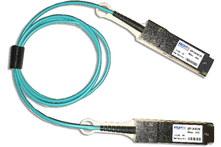
QSFP+ 40G AOC Cable
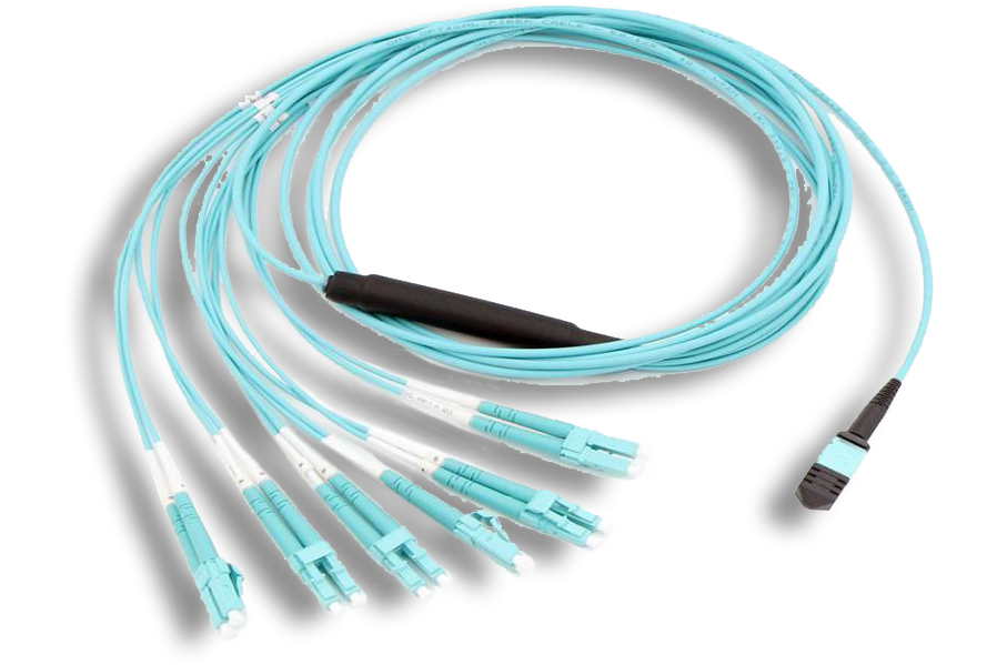
MTP/MPO Harness Assemblies
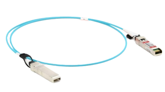
25G SFP28 AOC Cable
SFPP AT AOC Cable
100G to 25G Adapter
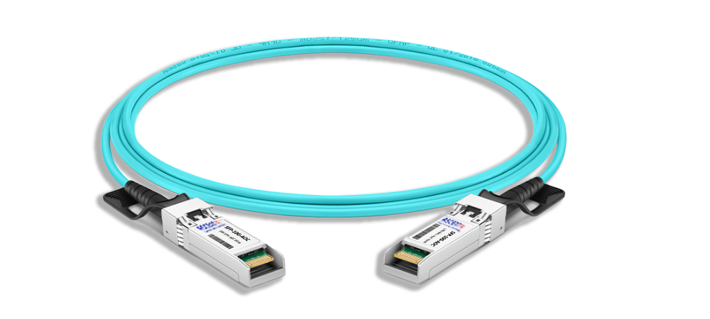
10G SFP+ Passive Copper Twinax Cable