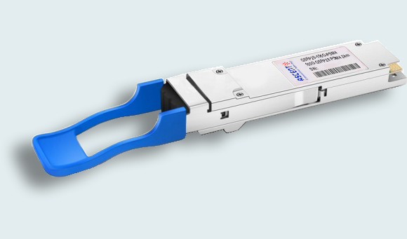
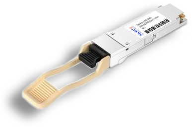
Ascent’s QSFP28 100G PSM4 transceiver module is designed to meet the requirements of optical fiber interface for 2 km reach over eight single-mode fibers.
• Hot Pluggable QSFP form factor
• Support 25.78125Gb/s per channel and 103.1Gb/s aggregate bit rate
• Power consumption < 3.5W
• 3.3V power supply voltage
• Case Operating Temperature: 0 °C to +70 °C
• Up to reach 2 km on Single-Mode MPO (APC 8-degree) connector receptacle
• 4 channels 1310 nm DFB
• 4 channels PIN photo detector array
• Internal CDR circuits on both receiver and transmitter channels
• RoHS-6 compliance
Absolute Maximum Ratings
Parameter | Symbol | Min. | Max. | Unit | Note |
Storage Temperature | TS | ‑40 | +95 | °C | |
Operating Case Temperature (Commercial) | TO | 0 | +70 | °C | |
Relative Humidity ‑ Storage | RHS | 0 | 95 | % | |
Relative Humidity ‑ Operating | RHO | 0 | 85 | % | |
Supply Voltage | VCC | ‑0.3 | 3.6 | V |
Operating conditions
Parameter | Symbol | Min | Typ. | Max | Unit | Note |
Operating Case Temperature | Tcase | 0 | ‑ | +70 | °C | |
DC Supply Voltage | VCC | 3.135 | ‑ | 3.465 | V | |
Module Supply Current | IIN | ‑ | ‑ | 1000 | mA |
Electrical Characteristics
Parameter | Symbol | Min. | Typ. | Max. | Unit | Note |
Transmitter | ||||||
Differential Data input Swing | VIN | 180 | ‑ | 900 | mV | |
Tx Differential Input Impendence | Zin | 90 | 100 | 110 | Ω | |
Tx Differential Output Impendence | Zout | 45 | 50 | 55 | Ω | |
ResetL Disable Voltage | Vr | 2.0 | ‑ | VCC+0.3 | V | |
ResetL Enable Voltage | VrEN | 0 | ‑ | 0.8 | V | |
ModSelL Disable Voltage | Vm | 2.0 | ‑ | Vcc+0.3 | V | |
ModSelL Enable Voltage | VmEN | 0 | ‑ | 0.8 | V | |
Receiver | ||||||
Differential Data Output Swing | VOUT | 180 | ‑ | 900 | mV | |
Rx Differential Output Impendence | ZOUT | 90 | 100 | 110 | Ω | |
IntL Assert Voltage | VInt | VCC‑0.5 | ‑ | VCC+0.3 | V | |
IntL De‑assert Voltage | VDInt | 0 | ‑ | +0.4 | V | |
Optical Specifications
Parameter | Symbol | Min. | Typ. | Max. | Units | Notes |
Transmitter | ||||||
Signal Rate each Lane | 25.78125 ppm ± 100ppm | Gbps | ||||
Lane Wavelength | L0 | 1295 | 1310 | 1325 | nm | |
L1 | 1295 | 1310 | 1325 | nm | ||
L2 | 1295 | 1310 | 1325 | nm | ||
L3 | 1295 | 1310 | 1325 | nm | ||
Side Mode Suppression Ratio | SMSR | 30 | dB | |||
Average Launch Power each Lane | Pavg | ‑9.4 | 2.0 | dBm | ||
Optical Modulation Amplitude each Lane | OMA | 2.2 | dBm | 1 | ||
Transmitter and Dispersion Penalty each Lane | TDP | 2.9 | dB | |||
Eye Mask Coordinates: X1, X2, X3, Y1, Y2, Y3 | {0.31, 0.4, 0.45, 0.34, 0.38, 0.4} | 2 | ||||
Average Launch Power of OFF Transmitter each Lane | ‑30 | dBm | ||||
Extinction Ratio | ER | 3.5 | dB | |||
Spectral Width (20 dB) | 1 | nm | ||||
Transmitter Reflectance | ‑12 | dB | ||||
Optical Return Loss Tolerance | 20 | dB | ||||
Receiver | ||||||
Signal Speed per Lane | 25.78125 ppm ± 100 ppm | Gbps | ||||
Lane Wavelength | L0 | 1295 | 1310 | 1325 | nm | |
L1 | 1295 | 1310 | 1325 | nm | ||
L2 | 1295 | 1310 | 1325 | nm | ||
L3 | 1295 | 1310 | 1325 | nm | ||
Damage Threshold each Lane | THd | 3.0 | dBm | 3 | ||
Average Receive Power each Lane | ‑12.66 | 2.0 | dBm | |||
Receiver Reflectance | ‑26 | dB | ||||
Sensitivity OMA each Lane [1] | Sen | ‑12.1 | dBm | 4 | ||
Stressed Receiver Sensitivity (OMA), each Lane | ‑8.8 | dBm | ||||
LOS Assert | LOSA | ‑18 | ||||
LOS De‑Assert | LOSD | ‑16 | ||||
LOS Hysteresis | LOSH | 0.5 | 3 | |||
Vertical Eye Closure Penalty | VECP | 1.9 | dB | 5 | ||
Stressed Eye J2 Jitter | J2 | 0.27 | UI | |||
Stressed Eye J4 Jitter | J4 | 0.39 | UI | |||
Notes:
1. Even if the TDP < 1 dB, the OMA min must exceed the minimum value specified here.
2. Hit ratio of 5E‑5, per IEEE.
3. The receiver shall be able to tolerate, without damage, continuous exposure to a modulated optical input signal having this power level on one lane. The receiver does not have to operate correctly at this input power.
4. Measured with conformance test signal at receiver input for BER = 5E‑5 BER.
5. Vertical eye closure penalty and stressed eye jitter are test conditions for measuring stressed receiver sensitivity. They are not characteristics of the receiver
Digital Diagnostics
Parameter | Symbol | Spec | Units | Condition/Notes |
Temperature | Te | ±3 | °C | |
Voltage | Vcc | ±5 % | V | |
IBias | BIAS | ±10 % | mA | |
Rx power | Rx‑pwr | ±2 | dBm | |
Tx power | Tx‑pwr | ±2 | dBm |

200G QSFP DD LR4 10km
200G QSFP56 SR4 850 nm 100 m

100G QSFP28 LX4 2km

100G QSFP28OA LR4 10km

100G QSFP28 ZR4 1310 nm 80 km
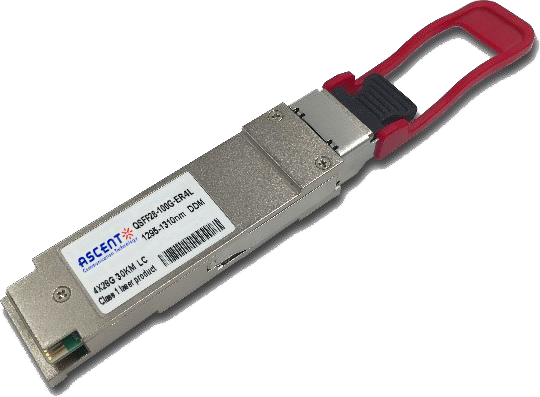
100G QSFP28 ER4L 1310 nm 40 km

100G QSFP28 ER4 1310 nm 40 km
100G QSFP28 LR4 1310 nm 10 km
100G QSFP28 LR Single λ 10 km

100G QSFP28 DR Single λ 500 m
100G QSFP28 CWDM4 1310 nm 2 km
100G QSFP28 SR4 850 nm 100 m
100G QSFP28 FR Single λ 1310 nm 2 km

100G QSFP28 SR01 BIDI MMF 850nm 100m

100G QSFP28 BIDI 80km

100G QSFP28 BIDI 40km

100G QSFP28 EZR4 100km

100G SFP56 ER1 30km

100G SFP56 LR1 10km
100G CFP2 ER4 40 km
100G CFP2 LR4 10 km
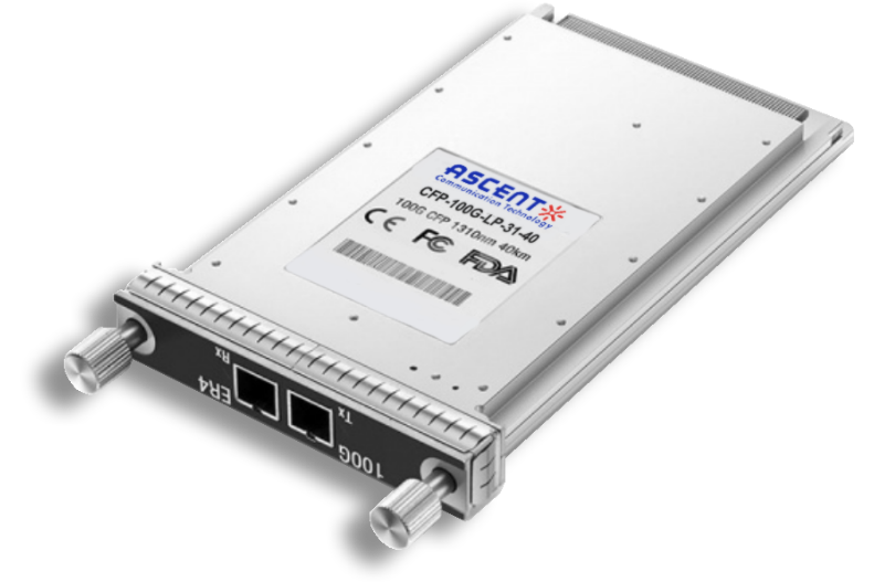
100G CFP ER4 40 km
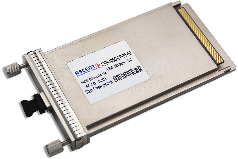
100G CFP LR4 10 km