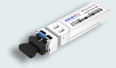
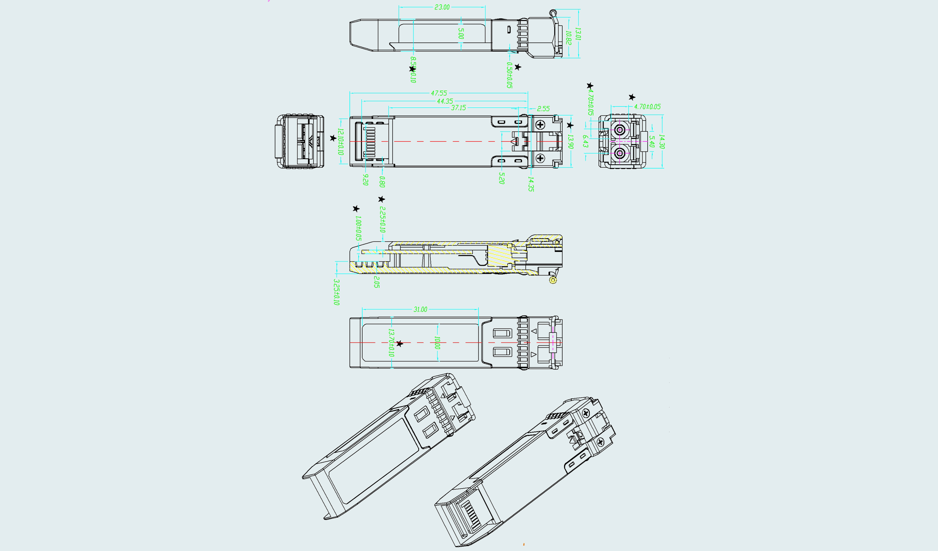
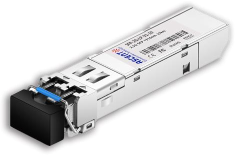
ASCENT’s SFP-AG-LP-31-10 Small Form Factor Pluggable (SFP) transceivers are compatible with the Small Form Factor Pluggable Multi-Sourcing Agreement (MSA). The transceiver consists of five sections: the LD driver, the limiting amplifier, the digital diagnostic monitor, the 1310nm FP laser and the PIN/TIA. The module data link up to 20 km in 9/125 µm Single-mode fiber. This transceiver meets the Small Form Pluggable (SFP) industry standard package utilizing an integral LC-Duplex optical interface connector. An enhanced Digital Diagnostic Monitoring Interface compliant with SFF-8472 has been incorporated into the transceiver. It allows real time access to the transceiver operating parameters such as transceiver temperature, laser bias current, transmitted optical power, and received optical power and transceiver supply voltage by reading a built-in memory with I2C interface. The optical output can be disabled by a LVTTL logic highlevel input of Tx Disable, and the system also can disable the module via I2C. Tx Fault is provided to indicate that degradation of the laser. Loss of Signal (LOS) output is provided to indicate the loss of an input optical signal of receiver or the link status with partner. The system can also get the LOS (or Link)/Disable/Fault information via I2C register access.
• Up to 1.25 Gb/s data links
• FP laser transmitter and PIN photo-detector
• Up to 10(20) km on 9/125 µm SMF
• Hot-pluggable SFP footprint
• Duplex LC/UPC type pluggable optical interface
• Low power dissipation
• Metal enclosure, for lower EMI
• RoHS compliant and lead-free
• Single +3.3 V power supply
• Supports Digital Diagnostic Monitoring interface
• Compliant with SFF-8472 and IEEE802.3z
• Switch to Switch Interface
• Gigabit Ethernet
• Switched Backplane Applications
• Router/Server Interface
• Other Optical Links
Parameter | Symbol | Min. | Typ. | Max. | Unit | Note |
Storage Temperature | TS | -40 | 85 | °C | ||
Storage Ambient Relative Humidity | HA | 0 | 85 | % | ||
Power Supply Voltage | VCC | -0.5 | 4 | V | ||
Signal Input Voltage | -0.3 | Vcc+0.3 | V | |||
Receiver Damage Threshold | +3 | dBm | ||||
Lead Soldering Temperature/Time | TSOLD | 260/10 | °C/sec | 1 | ||
Lead Soldering Temperature/Time | TSOLD | 360/10 | °C/sec | 2 |
Notes:
1. Suitable for wave soldering.
2. Only for soldering by iron.
Parameter | Symbol | Min. | Typ. | Max. | Unit | Note |
Operating Case Temperature | Tcase | 0 | +70 | °C | Commercial | |
-40 | +85 | °C | Industrial | |||
Ambient Humidity | HA | 5 | 70 | % | Non-condensing | |
Power Supply Voltage | VCC | 3.13 | 3.3 | 3.47 | V | |
Power Supply Current | Icc | 280 | mA | |||
Data Rate | 1250/1250 | Mbps | TX rate/RX rate | |||
Transmission Distance | 20 | km | ||||
Coupled Fiber | Single-mode fiber |
Specification of Transmitter
Parameter | Symbol | Min. | Typ. | Max. | Unit | Note |
Average Output Power | POUT | -9 | -3 | dBm | ||
Extinction Ratio | ER | 9 | dB | |||
Center Wavelength | λC | 1260 | 1310 | 1360 | nm | |
Spectrum Bandwidth (RMS) | σ | 3.5 | nm | FP Laser | ||
Transmitter OFF Output Power | POff | -45 | dBm | |||
Jitter p-p | tJ | 0.1 | UI | 1 | ||
Output Eye Mask | Compliant with IEEE802.3z (class 1 laser safety) | 2 | ||||
1. Measure at 27-1 NRZ PRBS pattern.
2. Transmitter eye mask definition.

Specification of Receiver
Parameter | Symbol | Min. | Typ. | Max. | Unit | Note |
Input Optical Wavelength | λIN | 1270 | 1610 | nm | ||
Receiver Sensitivity | PIN | -24 | dBm | 1 | ||
Input Saturation Power (Overload) | PSAT | -3 | dBm | |||
Loss of Signal Assert | PA | -45 | dBm | |||
Loss of Signal De-assert | PD | -24.5 | dBm | 2 | ||
LOS Hysteresis | PD-PA | 0.5 | 6 | dB |
Notes:
1. Measured with light source 1310 nm, ER = 9 dB; BER ≤ 10-12 @ PRBS = 27-1 NRZ
2. When LOS De-asserted, the RX data± output is signal output.

Digital Diagnostic Monitoring Information
Parameter | Unit | Accuracy |
Case Temperature | °C | ±3 |
Supply Voltage | V | ±3% |
Tx Bias Current | mA | ±10% |
Tx Optical Power | dB | ±3 |
Rx Optical Power | dB | ±3 |
Electrical Interface Characteristics
Parameter | Symbol | Min. | Typ. | Max. | Unit | Note |
Transmitter | ||||||
Total Supply Current | ICC | A | mA | 1 | ||
Transmitter Disable Input-High | VDISH | 2 | Vcc+0.3 | V | LVTTL | |
Transmitter Disable Input-Low | VDISL | 0 | 0.8 | V | LVTTL | |
Transmitter Fault Input-High | VTxFH | 2 | Vcc+0.3 | V | LVTTL | |
Transmitter Fault Input-Low | VTxFL | 0 | 0.8 | V | LVTTL | |
Receiver | ||||||
Total Supply Current | ICC | B | mA | 1 | ||
LOS Output Voltage-High | VLOSH | 2 | Vcc+0.3 | V | LVTTL | |
LOS Output Voltage-Low | VLOSL | 0 | 0.8 | V | LVTTL | |
Note 1: A (TX)+ B (RX) = 280 mA (Not include termination circuit)


2.5G SFP 1550nm 80km
2.5G SFP CWDM 40 km
2.5G SFP BiDi 10 km

2.5G SFP 1310nm 20km
2.5G SFP 1310nm 10km
2.5G SFP 1310 nm 2 km
1.25G SFP EZX 1550 nm 120 km
1.25G SFP ZX 1550 nm 80 km
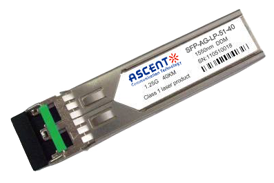
1.25G SFP EX 1550 nm 40 km
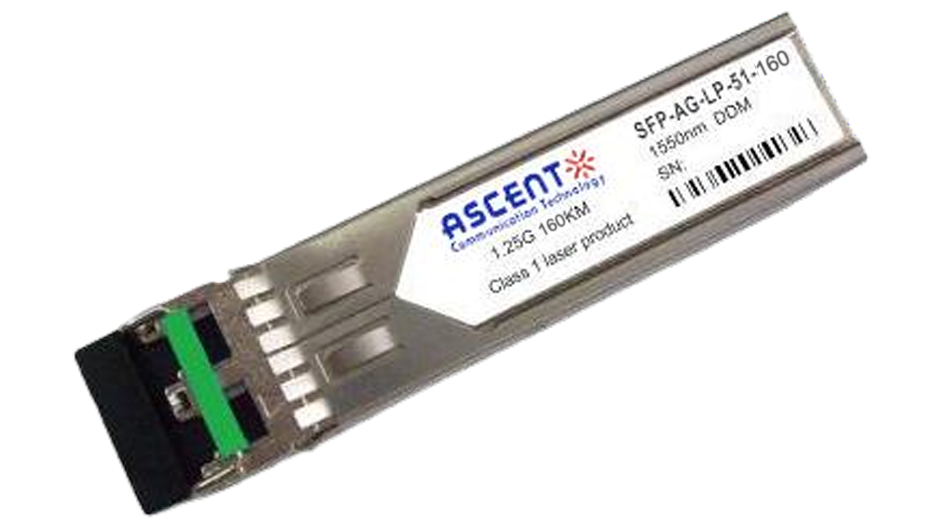
1.25G SFP 1550 nm 160 km
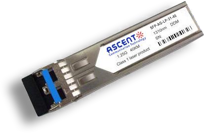
1.25G SFP EX 1310 nm 40 km
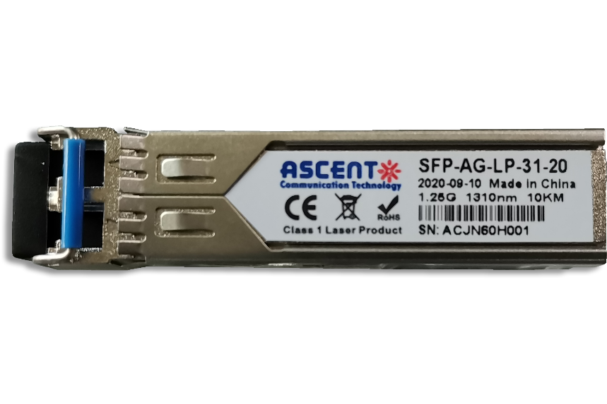
1.25G SFP 1310 nm 20 km

1.25G SFP SR 850 nm 550 m

1.25G SFP BX 3155 20 km
1.25G SFP BX 3155 3 km
1.25G SFP BX 4950 120 km

1.25G SFP BX 4950 80 km

1.25G SFP BX 3150 40 km
1.25G SFP BX 3149 20 km
1.25G SFP CWDM 4931 20 km

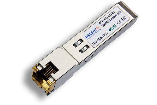
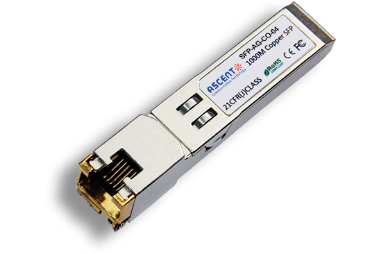
1000M Copper SFP
10/100/1000M Copper SFP

1000M Copper SFP w/ Auto-Negotiation
10/100/1000M Copper SFP w/ Link Indicator
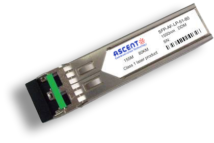
155M SFP 1550 nm 80 km

155M SFP OC3 1310nm 15 km