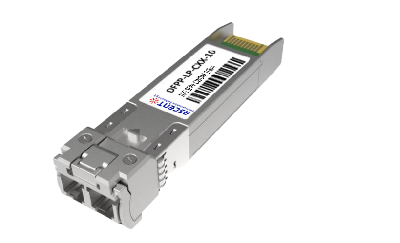
The DFPP-LP-CXX-10 is a high-performance 10G CWDM SFP+ transceiver engineered for optical data transmission and reception over single-mode fiber links up to 10 kilometers. Designed for demanding 10GBASE-LR applications, this module features a CWDM DFB laser and complies with SFI electrical specifications, ensuring robust signal integrity and minimal EMI through differential AC coupling and high-quality termination. The transceiver's transmitter section converts high-speed electrical data into optical signals, featuring an internal Automatic Power Control (APC) loop that maintains consistent optical output despite voltage or temperature changes. It includes important safety and diagnostic functions, such as TX_Disable and TX_Fault indicators, providing system-level control and real-time fault detection. These functions help ensure reliable operation and simplify integration into network equipment. On the receiving end, the module transforms incoming 10Gbps optical signals into PECL/CML electrical outputs, with a built-in Loss of Signal (Rx_LOS) feature that alerts the host system to degraded or absent signal conditions. This makes the DFPP-LP-CXX-10 ideal for ensuring high data integrity in long-reach optical links, helping identify issues such as disconnected cables or non-functioning transmitters. Overall, it offers a compact and efficient solution for CWDM optical networking with a strong emphasis on stability, reliability, and compliance with industry standards.
· 10Gb/s serial optical interface compliant to 802.3ae 10GBASE-LR
· Electrical interface compliant to SFF-8431
· Small Form Factor Pluggable compliant to SFF-8432
· LC Duplex connector
· CWDM DFB transmitter, PIN photo-detector
· 2-wire interface for management specifications compliant with SFF 8472 digital diagnostic monitoring interface for optical transceivers
· Low EMI
· Low power consumption
· Advanced firmware allow customer system encryption information to be stored in transceiver
· Cost effective SFP+ solution, enables higher port densities and greater bandwidth
· RoHS compliant
· Operating case temperature range:
Commercial: 0 to 70 °C
Industrial: -40 to 85 °C
Recommended Operating Conditions
Recommended Operating Environment specifies parameters for which the electrical and optical characteristics hold unless otherwise noted.
Parameter | Symbol | Min. | Typ. | Max. | Unit | Note |
Power Supply Voltage | Vcc | 3.135 | 3.3 | 3.465 | V | |
Power Supply Current | Icc | 350 | mA | |||
Operating Case Temperature | TC | 0 | 25 | 70 | °C | |
Relative Humidity | RH | 5 | 95 | % |
Optical Characteristics
Parameter | Values | Unit |
Operating Reach | 10 | km |
Transmitter | ||
Center Wavelength (Range) | 1391, 1411, 1431, 1451, 1471, 1491, 1511, 1531, 1551, 1571, 1591, 1611 | nm |
Side Mode Suppression Ratio (Min) | 30 | dB |
Output Power | 0 to 6 | dBm |
Average Launch Power | 0 to 6 | dBm |
Transmitter and Dispersion Penalty (Max) | 3.2 | dB |
Average Launch Power of OFF Transmitter (Max) | -30 | dBm |
Extinction Ratio (Min) | 3.5 | dB |
RIN12 OMA (Max) | -128 | dB/Hz |
Optical Return Loss Tolerance (min) | 12 | dB |
Receiver | ||
Center Wavelength (Range) | 1391, 1411, 1431, 1451, 1471, 1491, 1511, 1531, 1551, 1571, 1591, 1611 | nm |
Receive Overload (Max) in Average Power (Note 1) | 0.5 | dBm |
Receive Sensitivity (Min) in Average Power (Note 2) | -14.4 | dBm |
Receiver Reflectance (Max) | -12 | dB |
Los Assert (Min) | -30 | dBm |
Los Dessert (Max) | -15 | dBm |
Los Hysteresis(min) | 0.5 | dB |
Receive Electrical 3dB Upper Cutoff Frequency (Max) | 12.3 | dBm |
Receiver Power (Damage, Max) | +7 | dBm |
Notes:
1. Average optical power shall be measured using the methods specified in TIA/EIA-455-95.
2. Measured with a PRBS 231-1 test pattern, @ 10.3125 Gb/s, BER≤10-12.
3. Path penalty is intended as the power penalty of the interface between back-to-back and the maximum applied dispersion.
Electrical Characteristics
The following electrical characteristics are defined over the Recommended Operating Environment unless otherwise specified.
Parameter | Symbol | Min. | Typ. | Max. | Unit | Note |
Data Rate | 9.95 | 10.3125 | 11.3 | Gbps | ||
Power Consumption | 1.5 | mW | ||||
Transmitter | ||||||
Single Ended Output Voltage Tolerance | -0.3 | 4 | V | |||
C common Mode Voltage Tolerance | 15 | mV | ||||
Tx Input Diff Voltage | VI | 180 | 800 | mV | ||
Tx Fault | VoL | -0.3 | 0.4 | V | At 0.7mA | |
Data Dependent Input Jitter | DDJ | 0.1 | UI | |||
Data Input Total Jitter | TJ | 0.28 | UI | |||
Receiver | ||||||
Single Ended Output Voltage Tolerance | -0.3 | 4 | V | |||
Rx Output Diff Voltage | Vo | 300 | 850 | mV | ||
Rx Output Rise and Fall Time | Tr/Tf | 30 | ps | 20% to 80% | ||
Total Jitter | TJ | 0.7 | UI | |||
Deterministic Jitter | DJ | 0.42 | UI |
Control and Status I/O Timing Characteristics
Timing characteristics of control and status I/O are included in Pin Description table, which is also defined in SFF-8431.
Parameter | Symbol | Min. | Typ. | Max. | Unit | Note |
TX Disable Assert Time | t_off | 10 | μs | Time from rising edge of TX Disable to when the optical output falls below 10% of nominal | ||
TX Disable Negate Time | t_on | 1 | ms | Time from falling edge of TX Disable to when the modulated optical output rises above 90% of nominal | ||
Time to Initialize, including Reset of TX_Fault | t_init | 300 | ms | From power on or negation of TX Fault using TX Disable | ||
TX Fault Assert Time | t_fault | 100 | μs | Time from fault to TX fault on | ||
TX Disable to Reset | t_reset | 10 | μs | Time TX Disable must be held high to reset TX fault | ||
LOS Assert Time | t_loss_on | 100 | μs | Time from LoS state to RX LOS assert | ||
LOS Deassert Time | t_loss_off | 100 | μs | Time from non-LOS state to RX LOS deassert | ||
Rate-Select Change Time | t_ratesel | 10 | μs | Time from rising or falling edge of Rate Select input until receiver bandwidth is in conformance with appropriate specification | ||
Serial lD Clock Rate | t_serial_clock | 100 | kHz |
Digital Diagnostic Functions
The following digital diagnostic characteristics are defined over the Recommended Operating Environment unless otherwise specified. It is compliant to SFF8472 Rev10.2 with internal calibration mode. For external calibration mode please contact our sales stuff.
Parameter | Symbol | Min | Typ. | Max | Unit | Note |
Temperature Monitor Absolute Error | DMI_Temp | -3 | 3 | °C | Over operating temp | |
Laser Power Monitor Absolute Error | DMI_TX | -3 | 3 | dB | ||
RX Power Monitor Absolute Error | DMI_RX | -3 | 3 | dB | -7dBm to -20dBm range | |
Supply Voltage Monitor Absolute Error | DMI_VCC | -0.08 | 0.08 | V | Full operating range | |
Bias Current Monitor | DMI_Ibias | -10% | 10% | mA |

10G SFP+ LR 1310 nm 40 km

10G SFP+ LR 1310 nm 20 km
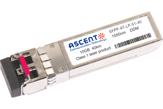
10G SFP+ LR 1310 nm 10 km
10G SFP+ LRM 1310 nm 2 km
10G SFP+ ER 1550 nm 40 km
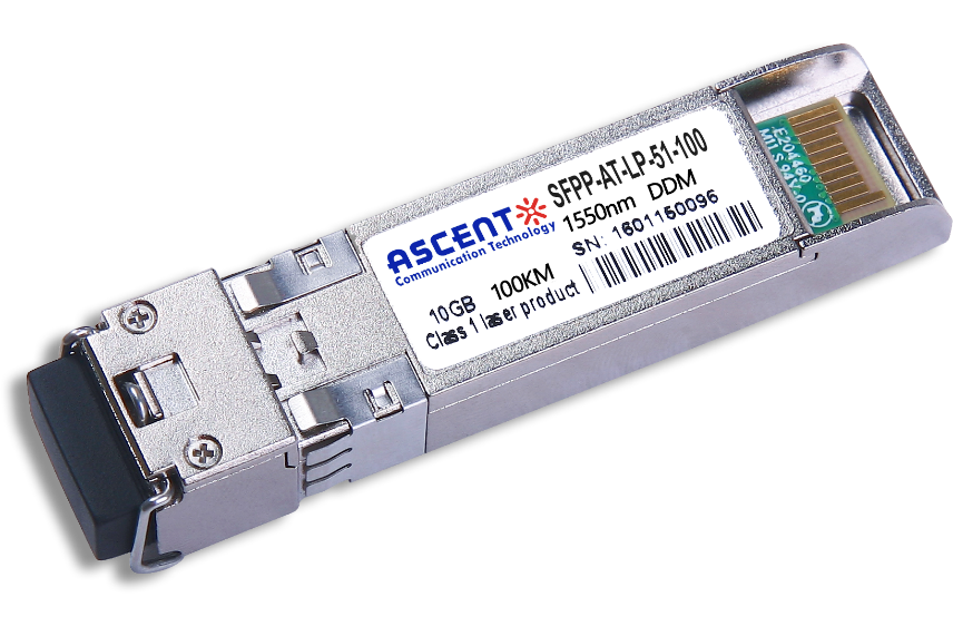
10G SFP+ CDR 1550 nm 100 km
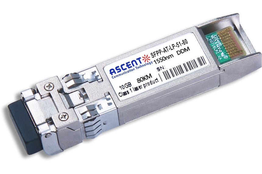
10G SFP+ ZR 1550 nm 80 km
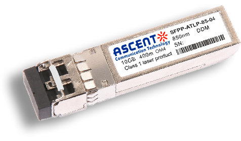
10G SFP+ 850 nm 400 m
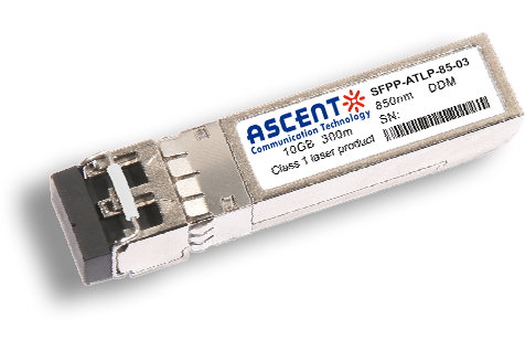
10G SFP+ 850 nm 300 m
10G SFP+ Tunable DWDM 80 km
10G SFP+ DWDM 80 km
10G SFP+ DWDM 40 km
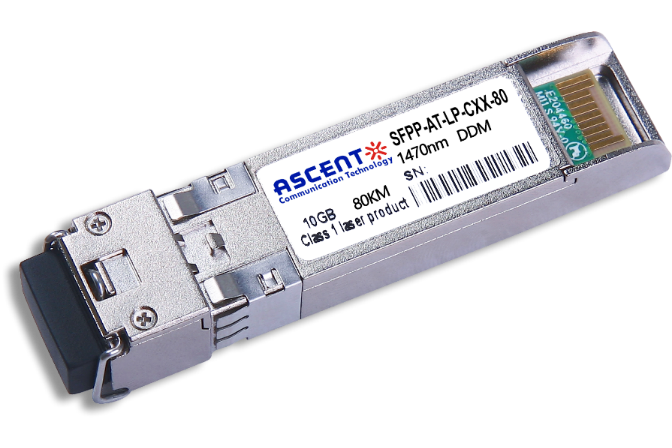
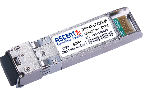
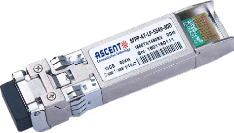
10G SFP+ CWDM 80 km
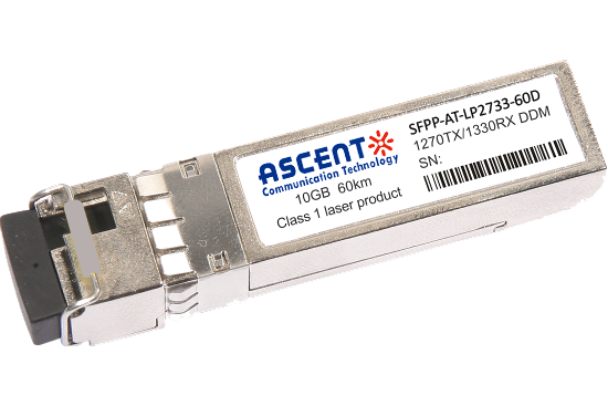
10G SFP+ CWDM 2733 60 km
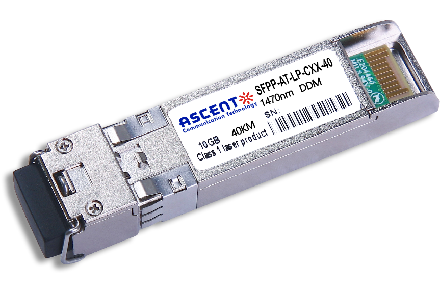
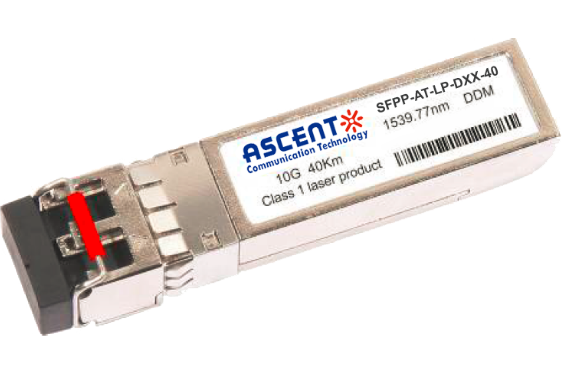
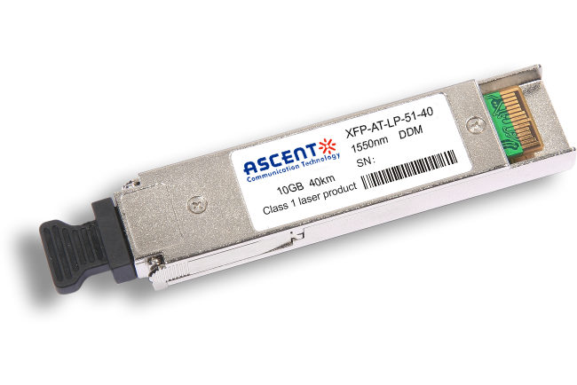
10G SFP+ CWDM 40 km
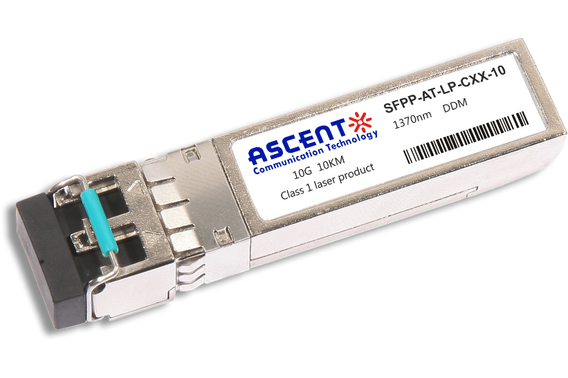
10G SFP+ Single mode CWDM 10 km
10G SFP+ CWDM 4955 80 km
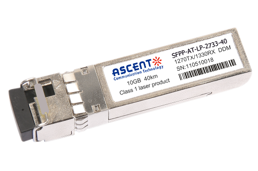
10G SFP+ CWDM 2733 40 km
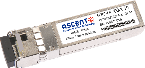
10G SFP+ CWDM 2733 10 km

10G XFP BIDI 80KM

10G XFP BIDI 40KM

10G XFP BIDI 20KM

10G XFP BIDI 10KM

10G XFP LR 1310 nm 20 km

10G XFP LR 1310 nm 10 km
10G XFP ER 1550 nm 40 km

10G XFP ZR 1550 nm 80 km
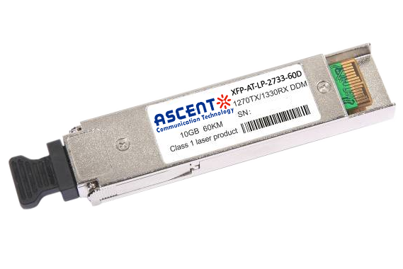
10G XFP CWDM 2633 60 km
10G SFP+ CWDM 1610 80 km
10G SFP+ Copper RJ45 30 m

10G X2 850nm 300m
16G SFP+ FC 850 nm 100 m
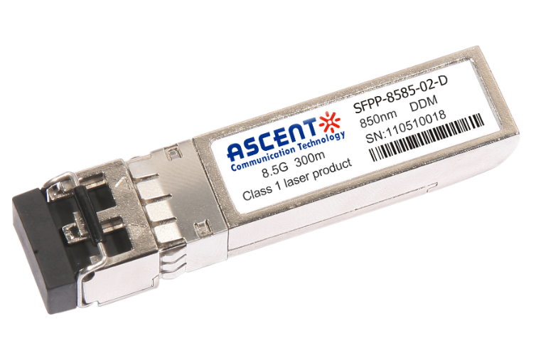
8.5G SFP+ SR 850 nm 150 m
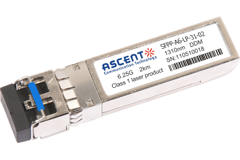
6.25G SFP+ LRM 1330 nm 2 km
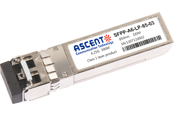
6.25G SFP+ SR 850 nm 300 m