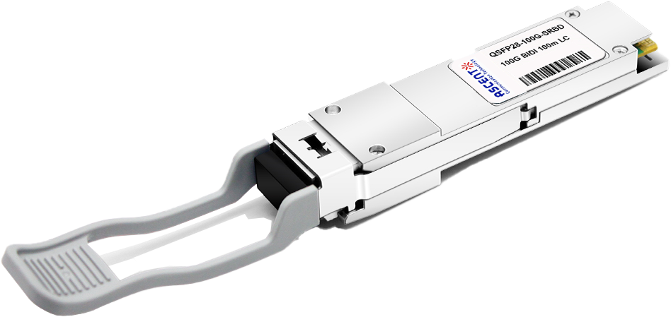
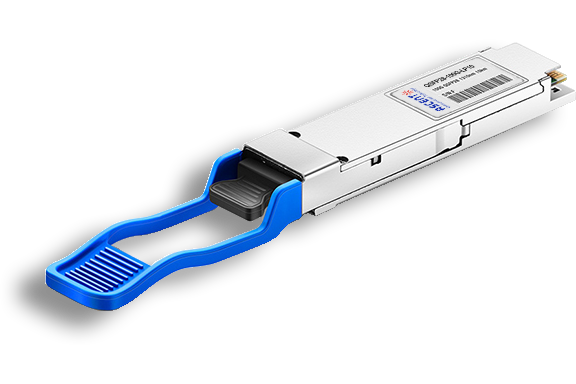
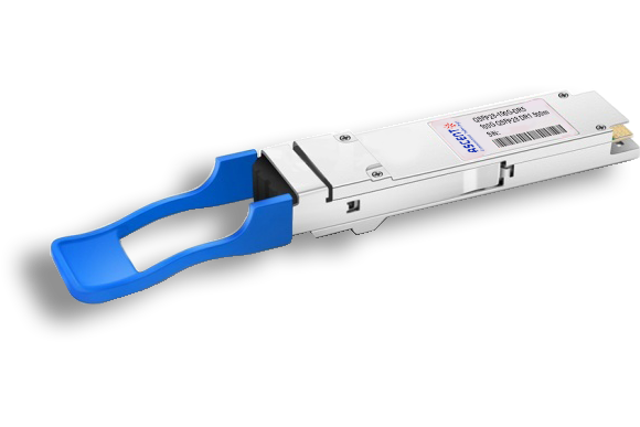
Ascent’s QSFP28 100G SR BIDI is a parallel Quad Small Form-factor Pluggable (QSFP28) Bi-Direction optical module which can support dual rate 40Gb/s and 100Gb/s bit rates in an optical communication application compliant to SFF-8636 standards. The module integrates four host electrical data into two optical lanes (by Dual Wavelength VCSEL Bi-Directional Optical Interface, 850nm and 900nm) to allow optical communication over a 2-fiber duplex LC optical multi-mode fiber. Reversely, on the receiver side, the module de-multiplexes 2 sets of optical input signal and converts them to 4 channels of electrical data. An optical fiber ribbon cable with an LC connector can be plugged into the QSFP28 module receptacle. Proper alignment is ensured by the guide pins inside the receptacle. The cable usually cannot be twisted for proper channel to channel alignment. Electrical connection is achieved through an MSA-compliant 38-pin edge type connector. The product is designed with form factor, optical/electrical connection, and digital diagnostic interface according to the QSFP+ Multi-Source Agreement (MSA). It has been designed to meet the harshest external operating conditions including temperature, humidity, and EMI interference.
· Compliant to the 100GbE XLPPI electrical specification per IEEE 802.3bm
· Compliant to QSFP28 SFF-8636 Specification
· Support 40GE/100GE aggregate bit rates
· Aggregate bandwidth of > 100Gbps
· Dual wavelength VCSEL bi-directional optical interface, PAM4 2 × 50-Gb/s 850nm/900 nm
· QSFP28 MSA compliant
· Capable of over 70m transmission on OM3 Multimode Fiber (MMF)and 100m on OM4 MMF
· Single +3.3V power supply operating
· With digital diagnostic functions
· Temperature range 0°C to 70°C
· RoHS Compliant Part
· Utilizes a standard LC duplex fiber cable allowing reuse of existing cable infrastructure
Parameter Storage Temperature | Symbol Ts | Min. -40 | Max. 85 | Unit °C | Notes
|
Supply Voltage | VCCT, R | -0.5 | 4 | V | |
Relative Humidity | RH | 0 | 85 | % |
Recommended Operating Conditions
Parameter Operating Case Temperature | Symbol Tc | Min. 0 | Typ. - | Max. 70 | Unit °C | Notes
|
Supply Voltage | VCCT, R | 3.13 | 3.3 | 3.47 | V | |
Supply Current | ICC | 1000 | mA | |||
Power Dissipation | PD | 3.5 | W |
Optical Characteristics (TOP = 0 to 70 °C, VCC = 3.0 to 3.6 Volts)
Parameter Transmitter | Symbol
| Min.
| Typ.
| Max.
| Unit | Notes
|
Optical Wavelength CH1 | λ | 832 | 850 | 868 | nm | |
Optical Wavelength CH2 | λ | 882 | 900 | 918 | nm | |
RMS Spectral Width | Pm | 0.5 | 0.65 | nm | ||
Average Optical Power per Channel | ||||||
Laser Off Power Per Channel | Poff | -30 | dBm | |||
Optical Extinction Ratio | ER | 3.0 | dB | |||
Relative Intensity Noise | Rin | -128 | dB/HZ | 1 | ||
Optical Return Loss Tolerance | 12 | dB | ||||
Receiver | ||||||
Optical Center Wavelength CH1 | λ | 882 | 900 | 918 | nm | |
Optical Center Wavelength CH2 | λ | 832 | 850 | 868 | nm | |
Receiver Sensitivity per Channel | R | -8 | dBm | |||
Maximum Input Power | PMAX | +0.5 | dBm | |||
Receiver Reflectance | Rrx | -15 | dB | |||
LOS De-Assert | LOSD | -10 | dBm | |||
LOS Assert | LOSA | -30 | dBm | |||
LOS Hysteresis | LOSH | 0.5 | dB | |||
Notes:
1. 12dB Reflection
Parameter | Symbol | Min. | Typ. | Max. | Unit | Notes |
Data Rate per Channel | 25.78125 | Gbps | ||||
Power Consumption | - | 2.5 | 3.5 | W | ||
Supply Current | Icc | 0.75 | 1.0 | A | ||
Control I/O Voltage-High | VIH | 2.0 | Vcc | V | ||
Control I/O Voltage-Low | VIL | 0 | 0.7 | V | ||
Inter-Channel Skew | TSK | 150 | Ps | |||
RESETL Duration | 10 | Us | ||||
RESETL De-assert time | 100 | ms | ||||
Power On Time | 100 | ms | ||||
Transmitter | ||||||
Single Ended Output Voltage Tolerance | 0.3 | 4 | V | 1 | ||
Common mode Voltage Tolerance | 15 | mV | ||||
Transmit Input Diff Voltage | VI | 120 | 1200 | mV | ||
Transmit Input Diff Impedance | ZIN | 80 | 100 | 120 | ||
Data Dependent Input Jitter | DDJ | 0.1 | UI | |||
Data Input Total Jitter | TJ | 0.28 | UI | |||
Receiver | ||||||
Single Ended Output Voltage Tolerance | 0.3 | 4 | V | |||
Rx Output Diff Voltage | Vo | 600 | 800 | mV | ||
Rx Output Rise and Fall Voltage | Tr/Tf | 12 | ps | 1 | ||
Total Jitter | TJ | 0.7 | UI | |||
Deterministic Jitter | DJ | 0.42 | UI | |||
Notes:
1. 20 to 80%
![]()
200G QSFP56 SR4 850 nm 100 m
100G QSFP28 ZR4 1310 nm 80 km
100G QSFP28 ER4 1310 nm 40 km
100G QSFP28 LR4 1310 nm 10 km

100G QSFP28 LR Single λ 10 km
100G QSFP28 CWDM4 1310 nm 2 km

100G QSFP28 PSM4 1310 nm 2 km
100G QSFP28 SR4 850 nm 100 m
100G QSFP28 FR Single λ 1310 nm 2 km
100G QSFP28 DR Single λ 500 m
100G CFP2 ER4 40 km
100G CFP2 LR4 10 km
100G CFP ER4 40 km
100G CFP LR4 10 km