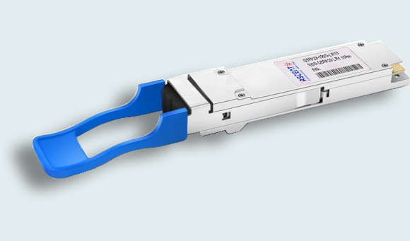
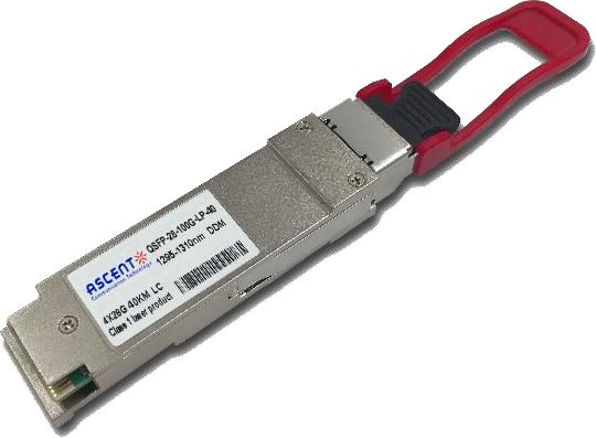
Ascent’s QSFP28 100G LR1 Ethernet module is a transceiver module designed for 10km optical communication applications, and it is compliant with IEEE 802.3cd and QSFP28 MSA standard.
• Compliant with QSFP28 Standard: SFF-8636 Rev 2.10a
• Compliant with IEEE802.3cu D3.2 100GBASE-LR1
• High speed I/O electrical interface (CAUI-4)
• Single 3.3V Supply Voltage
• Maximum power consumption 4.5W
• 0-70 ºC Case Operating Temperature
• 1311nm EML laser and PIN Receiver
• Hermetically sealed TO Based design
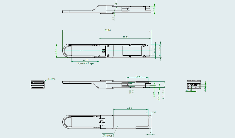
• QSFP28 MSA package with duplex LC connector
• Two Wire Serial Interface with Digital Diagnostic Monitoring
• KP4 FEC termination inside module
• Supporting 10km reach of single mode fiber
• Complies with EU Directive 2011/65/EU (RoHS compliant)
• Class 1 Laser
Parameter | Symbol | Min. | Typ. | Max. | Unit | Notes |
Storage Temperature | TS | ‑40 | ‑ | +85 | ºC | |
Supply Voltage | VCC | ‑0.3 | ‑ | 3.6 | V | |
Relative Humidity (Non‑Condensing) | RH | 5 | ‑ | 95 | % | |
Data Input Voltage – Differential | |VDIP‑VDIN| | ‑ | ‑ | 1.0 | V | |
Control Input Voltage | VI | ‑0.3 | ‑ | Vcc+0.3 | V | |
Control Output Current | IO | ‑20 | ‑ | 20 | mA |
Recommended Operating Conditions
Parameter | Symbol | Min. | Typ. | Max. | Unit | Note |
Operating Case Temperature | TOPR | 0 | ‑ | 70 | °C | |
Power Supply Voltage | VCC | 3.135 | 3.3 | 3.465 | V | |
Instantaneous Peak Current at Hot Plug | ICC_IP | ‑ | ‑ | 1800 | mA | |
Sustained Peak Current at Hot Plug | ICC_SP | ‑ | ‑ | 1485 | mA | |
Maximum Power Dissipation | PD | ‑ | ‑ | 4.5 | W | 1 |
Maximum Power Dissipation, Low Power Mode | PDLP | ‑ | ‑ | 1.5 | W | |
Signaling Rate | SR | ‑ | 53.125 | ‑ | GBd | |
Control Input Voltage High | VIH | VCC*0.7 | ‑ | VCC+0.3 | V | |
Control Input Voltage Low | VIL | ‑0.3 | ‑ | VCC*0.3 | V | |
Two Wire Serial Interface Clock Rate | ‑ | ‑ | ‑ | 400 | kHz | |
Power Supply Noise | ‑ | ‑ | ‑ | 66 | mVpp | 2 |
Rx Differential Data Output Load | ‑ | ‑ | 100 | ‑ | ohms | |
Operating Distance | ‑ | 2 | ‑ | 10000 | m |
Notes:
1. With power supply voltage 3.3 V.
2. 10Hz ‑10MHz
Optical and Electrical Characteristics
Parameter | Symbol | Min. | Typ. | Max. | Unit | Note |
Transmitter | ||||||
Wavelength | λC | 1304.5 | 1311 | 1317.5 | nm | |
Side Mode Suppression Ratio | SMSR | 30 | ‑ | ‑ | dB | |
Average Optical Launch Power | POUT | ‑1.9 | ‑ | 4.8 | dBm | 1 |
Average Launch Power of OFF Transmitter | POUT_OFF | ‑ | ‑ | ‑15 | dBm | |
Extinction Ratio | ER | 3.5 | ‑ | ‑ | dB | |
Outer Optical Modulation Amplitude | OMAouter | ‑ | ‑ | 5 | dBm | |
Outer Optical Modulation Amplitude for TDECQ <1.4 dB for 1.4 dB ≤TDECQ ≤3.4 dB | OMAouter |
1.1 ‑0.3+ TDECQ |
‑ ‑ |
‑ ‑ |
dBm dBm | |
Transmitter and Dispersion Eye Closure | TDECQ | ‑ | ‑ | 3.4 | dB | |
Transmitter eye closure for PAM4 (TECQ) | TECQ |
‑ |
‑ |
3.4 |
dB | |
|TDECQ ‑ TECQ| | ‑ | ‑ | ‑ | 2.5 | dB | |
Over/Under‑Shoot | ‑ | ‑ | ‑ | 22 | % | |
Transmitter Power Excursion | ‑ | ‑ | ‑ | 2.8 | dBm | |
RIN15.6OMA | RIN | ‑ | ‑ | ‑136 | dB/Hz | |
Optical return loss tolerance | ORLT | ‑ | ‑ | 15.6 | dB | |
Transmitter transition time | ‑ | ‑ | 17 | ps | ||
Transmitter reflectance | TR | ‑ | ‑ | ‑26 | dB | |
Receiver | ||||||
Wavelength | λC | 1304.5 | 1311 | 1317.5 | nm | |
Damage Threshold | 5.8 | ‑ | ‑ | dBm | ||
Average Receive Power | ‑8.2 | ‑ | 4.8 | dBm | 2 | |
Receive Power (OMAouter) | RP | ‑ | ‑ | 5 | dBm | |
Receiver Reflectance | RR | ‑ | ‑ | ‑26 | dB | |
Receiver Sensitivity (OMAouter) for TECQ < 1.4 dB for 1.4 dB≤ TECQ ≤3.4 dB | RS |
‑ ‑ |
‑ ‑ |
‑6.1 ‑7.5+ TECQ |
dBm dBm | |
Stressed Receiver Sensitivity | SRS | ‑ | ‑ | ‑4.1 | dBm | 3 |
Stressed Receiver Sensitivity Test Conditions | ||||||
Stressed eye closure for PAM4 (SECQ) | SECQ | ‑ | ‑ | 3.4 | dB | |
Notes:
1. Average launch power is informative and not the principal indicator of signal strength.
2. Average receive power (min) is informative and not the principal indicator of signal strength.
3. Measured with conformance test signal at TP3 for the BER = 2.4 x 10‑4.
Electrical Specifications High Speed Signal
Compliant with IEEE 802.3 CAUI‑4
Parameter | Symbol | Min. | Typ. | Max. | Unit | Note |
Receiver (Module Output) | ||||||
AC Common‑Mode Output Voltage (RMS) | ‑ | ‑ | 17.5 | mV | ||
Differential Output Voltage | ‑ | ‑ | 900 | mV | ||
Eye Width | 0.57 | ‑ | ‑ | UI | ||
Eye Height Differential | 228 | ‑ | ‑ | mV | ||
Vertical Eye Closure | ‑ | ‑ | 5.5 | dB | ||
Differential Termination Mismatch | ‑ | ‑ | 10 | % | ||
Transition Time (20% to 80%) | 12 | ‑ | ‑ | ps | ||
DC Common Mode Voltage | ‑350 | ‑ | 2850 | mV | ||
Transmitter (Module Input) | ||||||
Differential pk‑pk Input Voltage Tolerance | 900 | ‑ | ‑ | mV | ||
Differential Termination Mismatch | ‑ | ‑ | 10 | % | ||
Single‑Ended Voltage Tolerance Range | ‑0.4 | ‑ | 3.3 | V | ||
DC Common Mode Voltage | ‑350 | ‑ | 2850 | mV | ||
Electrical Specification Low Speed Signal
Compliant with SFF‑8679 Rev 1.8
Parameter | Symbol | Min. | Max. | Unit | Condition |
Module Output SCL and SDA | VOL | 0 | 0.4 | V | |
VOH | Vcc‑0.5 | Vcc+0.3 | V | ||
Module Input SCL and SDA | VIL | ‑0.3 | Vcc*0.3 | V | |
VIH | Vcc*0.7 | Vcc+0.5 | V | ||
LPMode/TxDis, ResetL, and ModSelL | VIL | ‑0.3 | 0.8 | V | |
VIH | 2 | Vcc+0.3 | V | ||
ModPrsL and IntL/RxLOSL | VOL | 0 | 0.4 | V | |
VOH | Vcc‑0.5 | Vcc+0.3 | V |
Digital Diagnostics
Parameter | Range | Accuracy | Unit | Calibration |
Temperature | 0 to 70 | ±3 | °C | Internal |
Voltage | 0 to VCC | ±3% | V | Internal |
Tx Bias Current | 0 to 100 | ±10% | mA | Internal |
Tx Output Power | ‑1.9 to +4.8 | ±3 | dB | Internal |
Rx Receive Power | ‑8.2 to +4.8 | ±3 | dB | Internal |

200G QSFP56 SR4 850 nm 100 m
100G QSFP28 ZR4 1310 nm 80 km
100G QSFP28 ER4 1310 nm 40 km
100G QSFP28 LR4 1310 nm 10 km
100G QSFP28 CWDM4 1310 nm 2 km

100G QSFP28 PSM4 1310 nm 2 km
100G QSFP28 SR4 850 nm 100 m
100G QSFP28 SR01 BIDI MMF 850nm 100m
100G QSFP28 FR Single λ 1310 nm 2 km
100G QSFP28 DR Single λ 500 m
100G CFP2 ER4 40 km
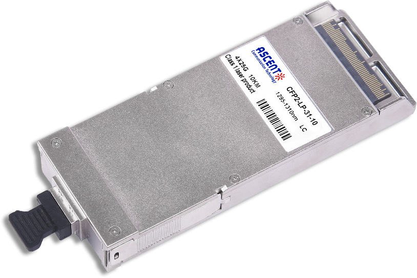
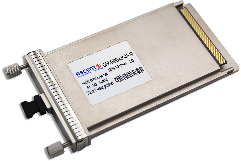
100G CFP2 LR4 10 km
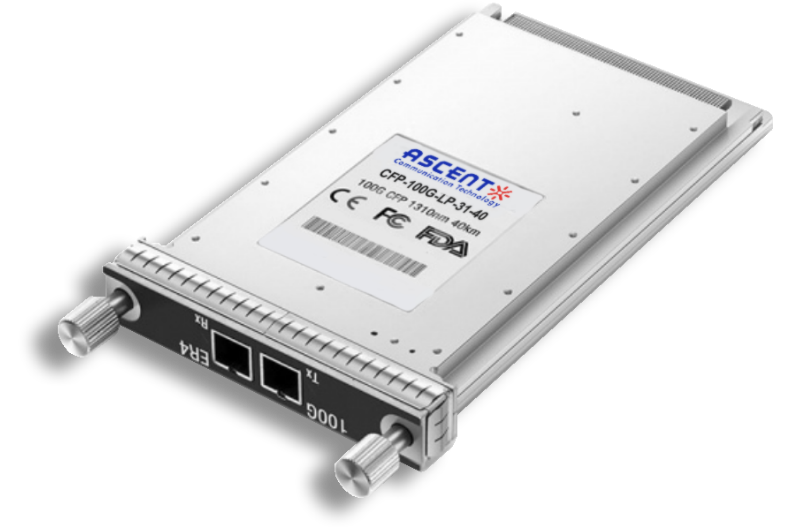
100G CFP ER4 40 km
100G CFP LR4 10 km