- FIBER OPTIC TRANSCEIVERS >800G & 400G Transceivers >800G OSFP DR8 1310 nm 500 m
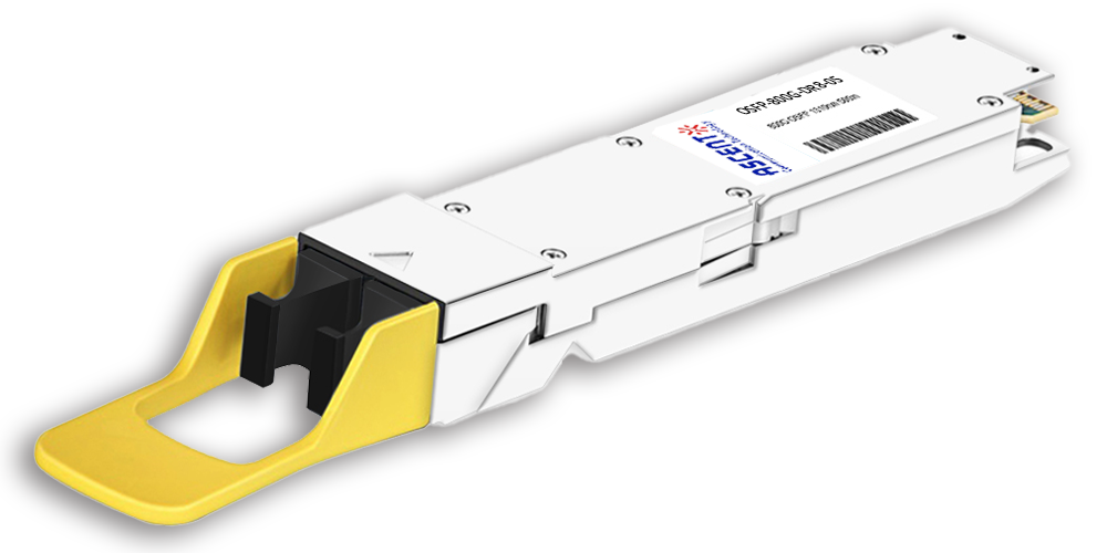
800G OSFP DR8 1310 nm 500 m
Ascentãs OSFP-800G-DR8-05 transceiver module is designed for use in 800 Gigabit Ethernet links over 500m single mode fiber. The module has 8 independent electrical input/output channels operating up to 106.25Gbps per channel. This transceiver consists of two transmitter/receiver units, with each operating on a set of wavelengths on the ITU G.694.2 CWDM at 1310nm. The transmitter path of the module incorporates a bi-directional PAM4 re-timer ASIC integrated with EML laser and 8-channel internal driver. On the receiver path, used 8 photodiodes and two 4-channel TIA arrays, along with the PAM4 re-timer. This transceiver is compliant with lEEE P802.3ck, IEEE 802.3cu, OSFP MSA. The built-in digital diagnostics monitoring (DDM) allows access to real-time operating parameters.
ã 0 to 500m over SMF with KP4 FEC supported at the Host side
ã Dual MPO-12 connector
ã Support multi-rate operation
ã Programmable Rx output pre-cursor EML 1310nm transmitter
ã PIN and TIA array on the receiver side
ã Power consumption < 16W
ã Case temperature range: 0ô¯C to 70ô¯C (commercial)
ã Safety Certification: TUV/UL/FDA*1
ã RoHS Compliant
Absolute Maximum Ratings
Exceeding the absolute maximum ratings table may cause permanent damage to the device. This is just an emphasized rating, and does not involve the functional operation of the device that exceeds the specifications of this technical specification under these or other conditions. Long-term operation under absolute maximum ratings will affect the reliability of the device.
Parameter | Symbol | Min. | Typ. | Max. | Unit |
Storage Temperature | Ts | -40 | +85 | ô¯C | |
3.3 V Power Supply Voltage | Vcc | -0.5 | 3.3 | 3.6 | V |
Data Input Voltage ã Single Ended | -0.5 | Vcc+0.5 | V | ||
Data Input Voltage ã Differential*1 | 0.8 | V | |||
Relative Humidity | RH | 5 | 95 | % |
Notes:
1. This is the maximum voltage that can be applied across the differential inputs without damaging the input circuitry. The damage threshold of the module input shall be at least 1600 mV peak to peak differential.
Recommended Operating Conditions*1
For operations beyond the recommended operating conditions, optical and electrical characteristics are not defined, reliability is not implied, and such operations for a long time may damage the module.
Parameter | Symbol | Min. | Typ. | Max. | Unit |
Operating Case Temperature*2 | Tc | 0 | 70 | ô¯C | |
Storage Temperature | Ts | -40 | +85 | ô¯C | |
Power Supply Voltage | Vcc | 3.135 | 3.3 | 3.465 | V |
Operating Relative Humidity | RH | 65 | % | ||
Power Consumption | PD | 16 | W | ||
Electrical Signal Rate per Channel (PAM encoded)*3 | 53.125 | GBd | |||
Optical Signal Rate per Channel (PAM encoded)*4 | 53.125 | GBd | |||
Power Supply Noise*5 | 66 | mVpp | |||
Receiver Differential Data Output Load | 100 | Ohm | |||
Fiber Length (9um SMF)*6 | 500 | m |
Notes:
1. Power Supply specifications, Instantaneous, sustained and steady state current compliant with OSFP MSA Power Classification.
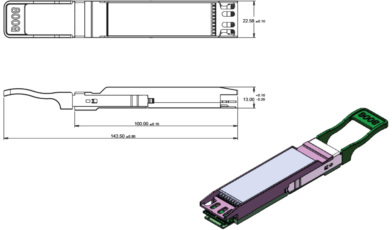
2. The position of case temperature measurement is shown in below figure.

3. 800GAUI-8 operation with Host generated FEC. The transmitter must receive pre-coded FEC signals from the host ASIC.
4. 8û100G DR operation with Host generated FEC. The transmitter must receive pre-coded FEC signals from the host ASIC.
5. Power Supply Noise is defined as the peak-to-peak noise amplitude over the frequency range at the host supply side of the power supply filter with the module and filter in place. Voltage levels including peak-to-peak noise are limited
to the recommended operating range of the associated power supply. See figure of power supply filter.
6. 9ö¥m SMF. The maximum link distance is based on an allocation of 3dB of attenuation and 3dB total connection and splice loss. The loss of a single connection shall not exceed 0.5dB.
Electrical Characteristics
Unless otherwise stated, the following characteristics are defined under recommended operating conditions.
Parameter | Symbol | Min. | Typ. | Max. | Unit |
Transceiver Power Consumption | 16 | W | |||
Transceiver Power Supply Current, Total | 5110 | mA | |||
AC coupling capacitors (Internal) | 0.1 | uF |
1. For control signal timing including LPWn/PRSn, INT/RSTn, SCL and SDA see Control Interface Section.
Reference Points
Symbol | Description |
TP0 to TP5 | The channel including the transmitter and receiver differential controlled impedance printed circuit board insertion loss and the cable assembly insertion loss. |
TP1 to TP4 | All cable assembly measurements are made between TP1 and TP4 as illustrated in IEEE 802.3ck 100GBASE-CR1, 200GBASE-CR2 or 400GBASE-CR4 link figure. |
TP0 to TP2 TP3 to TP5 | A mated connector pair has been included in both the transmitter and receiver specifications defined in 802.3ck 162.9.3 and 162.9.4. The recommended maximum insertion loss from TP0 to TP2 or from TP3 to TP5 including the test fixture is provided in 802.3ck 162.9.3.2 |
TP2 | Unless specified otherwise, all transmitter measurements defined in 802.3ck 162.9.3 are made at TP2 utilizing the test fixture specified in Annex 162B. |
TP3 | Unless specified otherwise, all receiver measurements and tests defined in 802.3ck 162.9.4 are made at TP3 utilizing the test fixture specified in Annex 162B. |
IEEE 802.3ck 100GBASE-CR1, 200GBASE-CR2 or 400GBASE-CR4 link

IEEE 802.3ck 400GAUI-4 compliance points TP1a, TP4a

IEEE 802.3ck 400GAUI-4 compliance points TP1, TP4

High Speed Electrical Input Characteristics
Unless otherwise stated, the following characteristics are defined under recommended operating conditions.
Parameter | Symbol | Min. | Typ. | Max. | Unit | Conditions |
Signaling Rate, Per Lane (PAM4 encoded) | TP1 | 53.125 | GBd | +/- 100 ppm | ||
Differential Peak-Peak Input Voltage Tolerance | TP1a | 750 | mV | |||
AC Common-Mode RMS Voltage Tolerance | TP1a | 25 | mV | |||
Differential-Mode to Common-Mode Return Loss Effective Return Loss, ERL | TP1 | Equation (120Gã2) | dB | |||
TP1 | 8.5 | dB | ||||
Differential Termination Mismatch | TP1 | 10 | % | |||
Module Stressed Input Tolerance | TP1a | See 120G.3.4.3 | 802.3ck | |||
Single-Ended Voltage Tolerance Range | TP1a | -0.4 | 3.3 | V | ||
DC Common-Mode Voltage Tolerance Range | TP1 | -350 | 2850 | mV | ||
Module Stressed Input Tolerance Test | ||||||
Pattern Generator Transition Time | 9 | ps | ||||
Applied Peak-Peak Sinusoidal Jitter | Table 162-16 | 802.3ck | ||||
Eye Height | 10 | mV | ||||
Vertical Eye Closure, VEC | 12 | 12.5 | dB | |||
Crosstalk Differential Peak-to-Peak Voltage | 845 | mV | ||||
Crosstalk Transition Time | 8.5 | ps | ||||
High Speed Electrical Output Characteristics
The following characteristics are defined over the Recommended Operating Conditions unless otherwise noted.
Parameter | Symbol | Min. | Typ. | Max. | Unit |
Signaling Rate, Per Lane (range) | TP4 | 53.125*1 ôÝ 100 ppm | GBd | ||
AC Common-Mode Output Voltage | TP4 | 25 | mV | ||
Differential Peak-to-Peak Input Voltage Short Mode Long mode | TP4 | 600 845 | |||
Eye Height Vertical Eye Closure | TP4 | 15 | |||
TP4 | 12 | ||||
Effective Return Loss | TP4 | 8.5 | |||
Common-Mode to Differential-Mode Return Loss | TP4 | Equation (120Gã1) | dB | ||
Differential Termination Mismatch | TP4 | 10 | % | ||
Transition Time | TP4 | 8.5 | ps | ||
DC Common-Mode Voltage Tolerance | TP4 | -0.35 | 2.85 | V | |
Notes:
1. The signaling rate range is derived from the PMD receiver input.
Optical Characteristics @TP2
Parameter | Symbol | Min. | Typ. | Max. | Unit |
Signaling Speed per Lane | 106.25 | Gbps | |||
Modulation Format | PAM4 | ||||
Center Wavelength | ö£ | 1304.5 | 1311 | 1317.5 | nm |
Side-Mode Suppression Ratio | SMSR | 30 | dB | ||
Extinction Ratio | ER | 3.5 | dB | ||
Average Launch Power*1 | -2.9 | 4 | dBm | ||
OMAouter per Lane | -0.8 | 4.2 | dBm | ||
Launch Power in OMAouter-TDECQ | -2.2 | dBm | |||
TDECQ (PAM4) | 3.4 | dB | |||
RIN21.4 OMA | -136 | dB/Hz | |||
Average Launch Power of OFF Transmitter | -15 | dBm | |||
Optical Return Loss Tolerance | 21.4 | dB | |||
Transmitter Reflectance | -26 | dB |
Notes:
1. Average launch power, each lane (min) is informative and not the principal indicator of signal strength.
A transmitter with launch power below this value cannot be compliant; however, a value above this
does not ensure compliance.
Optical Characteristics @TP3
Parameter | Symbol | Min. | Typ. | Max. | Unit |
Signaling Speed per Lane | 106.25 | Gbps | |||
Center Wavelength | ö£ | 1305.5 | 1311 | 1317.5 | nm |
Damage Threshold | 5 | dBm | |||
Average Receiver Power per Lane | -5.9 | 4 | dBm | ||
Saturation Receive Power (OMAouter) per Lane | 4.2 | dBm | |||
Unstressed Receiver Sensitivity (OMAouter) per Lane | Sen*1 | -4.4 | dBm | ||
LOS Assert (Avg.) | LOSA | -15 | dBm | ||
LOS De-Assert (Avg.) | LOSD | -10 | dBm | ||
RSSI Accuracy | -2 | +2 | dB | ||
Receiver Reflectance | -26 | dB |
Notes:
1. Receiver sensitivity (OMAouter), each lane (max) is informative and is defined for a transmitter with TDECQ of 0.9 dB.
Regulatory Compliance Issues
Various standard and regulations apply to the OSFP-800G-DR8-05 modules. These include eye-safety, Component Recognition, RoHS, ESD, EMC and Immunity.
Please note the transmitter module is a Class 1 laser product. See Regulatory Compliance Table for details.
Regulatory Compliance Table
Feature | Test Method | Performance |
Laser Eye Safety and Equipment Type Testing
| (IEC) EN 62368-1:2014+A11 (IEC) EN 60825-1:2014 (IEC) EN 60825-2:2004+A1+A2 | CDRH Accession Number:2132182-000 TUV File: R 50457725 0001 CB File: JPTUV-100513 |
Component Recognition | Underwriters Laboratories (UL) and Canadian Standards Association (CSA) Joint Component Recognition for Information Technology Equipment including Electrical Business Equipment | UL File: E317337 |
RoHS Compliance | RoHS Directive 2011/65/EU&(EU)2015/863 | Less than 100 ppm of cadmium. Less than 1000 ppm lead, mercury, hexavalent chromium, poly brominated biphenyls (PPB), poly brominated biphenyl ethers (PBDE), dibutyl phthalate, butyl benzyl phthalate, bis (2-ethylhexyl) phthalate and diisobutyl phthalates. |
Electrostatic Discharge (ESD) to the Electrical Contacts | JEDEC Human Body Model (HBM) | High speed contacts shall withstand 1000V. All other contacts shall withstand 2000 V. |
Electrostatic Discharge (ESD) to the Optical Connector Receptacle | IEC 61000-4-2:2008 | When installed in a properly grounded housing and chassis the units are subjected to 15kV air discharges during operation and 8kV direct discharges to the case. |
Electromagnetic Interference (EMI) | FCC Part 15 Class B; CISPR 32 (EN55032) 2015; | System margins are dependent on customer board and chassis design. |
Immunity | IEC 61000-4-3:2010; EN55035:2017 | Typically shows no measurable effect from a 10V/m field swept from 80 MHz to 6 GHz applied to the module without a chassis enclosure. |

Electrostatic Discharge (ESD)
The OSFP-800G-DR8-05 is complies with the ESD requirements described in the Regulatory Compliance Table. However, in the normal processing and operation of optical transceiver, the following two types of situations need special attention.
Case I: Before inserting the transceiver into the rack meeting the requirements of OSFP compliant cage, ESD preventive measures must be taken to protect the equipment. For example, the grounding wrist strap, workbench and floor should be used wherever the transceiver is handled.
Case II: After the transceiver is installed, the electrostatic discharge outside the chassis of the host equipment shall be within the scope of system level ESD requirements. If the optical interface of the transceiver is exposed outside the host equipment cabinet, the transceiver may be subject to equipment system level ESD requirements.
Electromagnetic Interference (EMI)
Communication equipment with optical transceivers is usually regulated by FCC in the United States and CENELEC EN55032 (CISPR 32) in Europe. The compliance of OSFP-800G-DR8-05 with these standards is detailed in the regulatory compliance table. The metal shell and shielding design of OSFP-800G-DR8-05 will help equipment designers minimize the equipment level EMI challenges they face
Flammability
OSFP-800G-DR8-05 optical transceiver meets UL certification requirements, its constituent materials have heat and corrosion resistance, and the plastic parts meet UL94V-0 requirements.

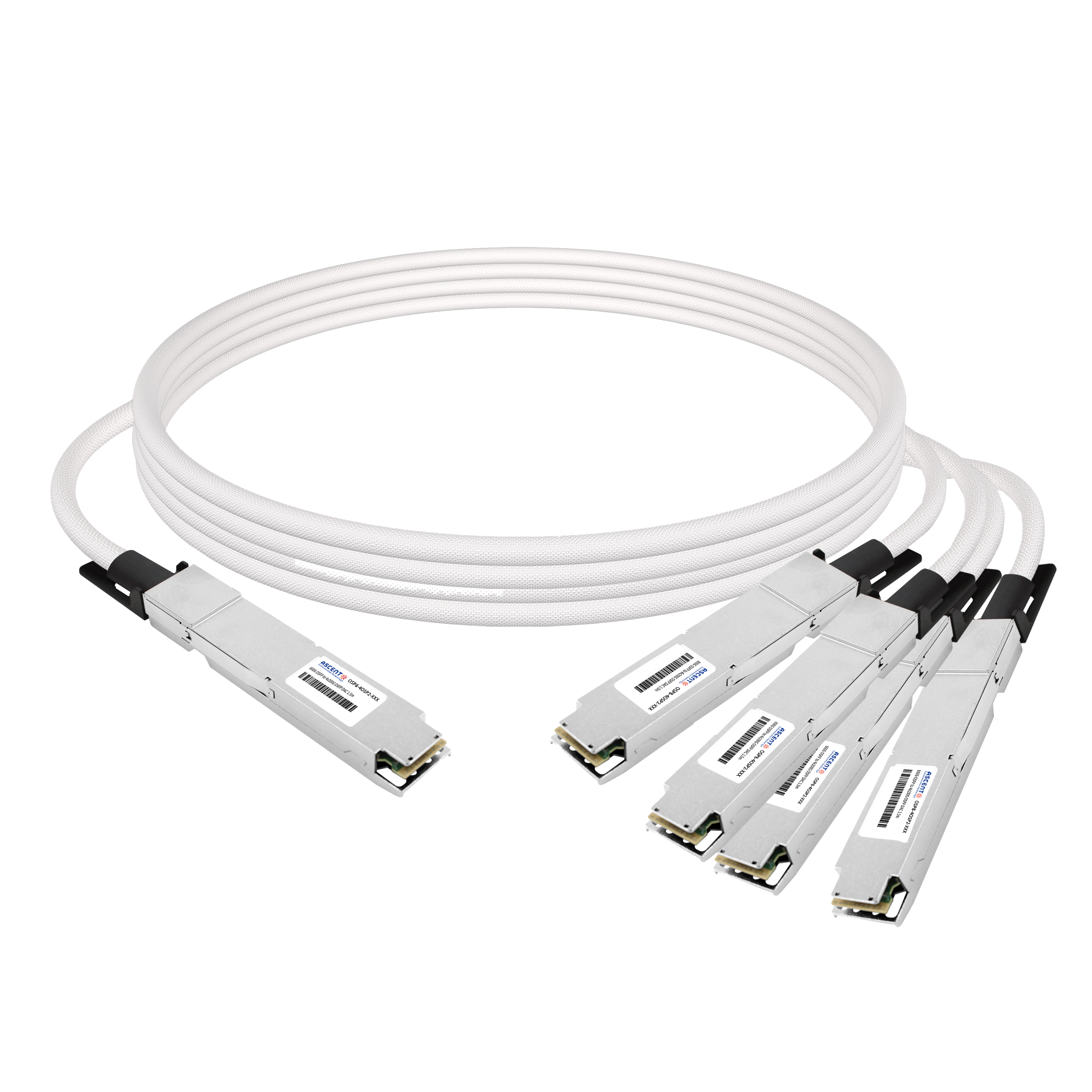
800G OSFP DAC Cable
800G IB NDR OSFP to 4xOSFP RHS Hairtail+ Direct Attach Copper Cable
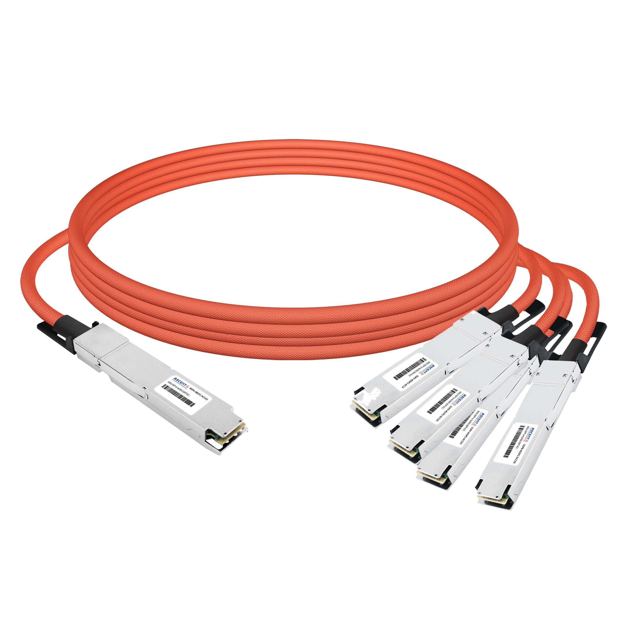
800G OSFP ACC Cable
800G OSFP Breakout to 4x200G OSFP Active Copper Cable
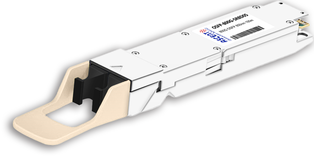
800G OSFP SR8 850 nm 100 m
OSFP-800G-SR8D-01 800 Gb/s OSFP SR8 850 nm 100 m Transceiver
400G QSFP56-DD 10km
400G QSFP-DD 4X100G LR1 Optical Transceiver
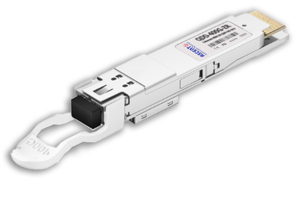
400G QSFP-DD ZR+
QSFP-DD-ZR-80 400 Gb/s QSFP-DD 80 km Transceiver
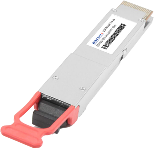
400G QSFP-DD ER8 40 km
QSFP-DD-ER8-40 400 Gb/s QSFP-DD 40 km Transceiver
400G QSFP-DD 40 km
400 Gb/s QSFP-DD 40 km Transceiver
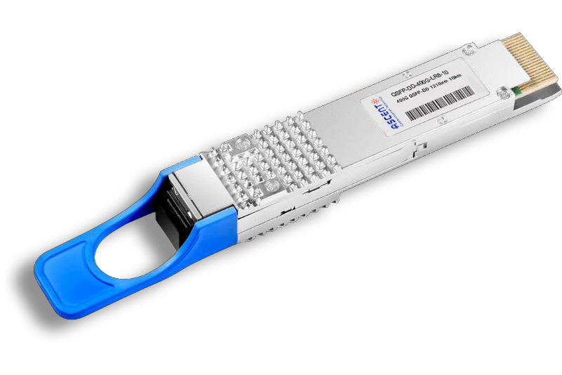
400G QSFP-DD LR8 1310 nm 10 km
QSFP-DD-LR8-10 400 Gb/s QSFP-DD LR8 10 km Transceiver

400G QSFP-DD LR4 CWDM 10 km
QSFP-DD-LR4-10 400 Gb/s QSFP-DD LR4 CWDM 10 km Transceiver
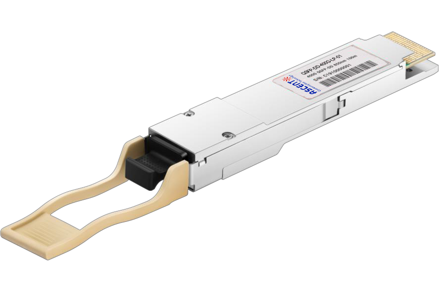
400G QSFP-DD SR8 850 nm 100 m
QSFP-DD-LP-01 400 Gb/s QSFP-DD SR8 100 m Transceiver
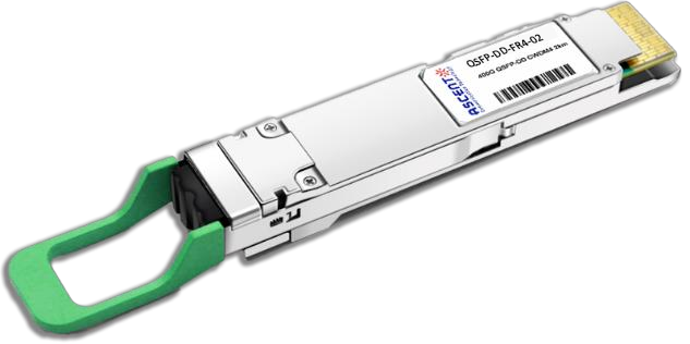
400G QSFP-DD FR4 2km
400 Gb/s QSFP-DD FR4 2 km DDM Transceiver
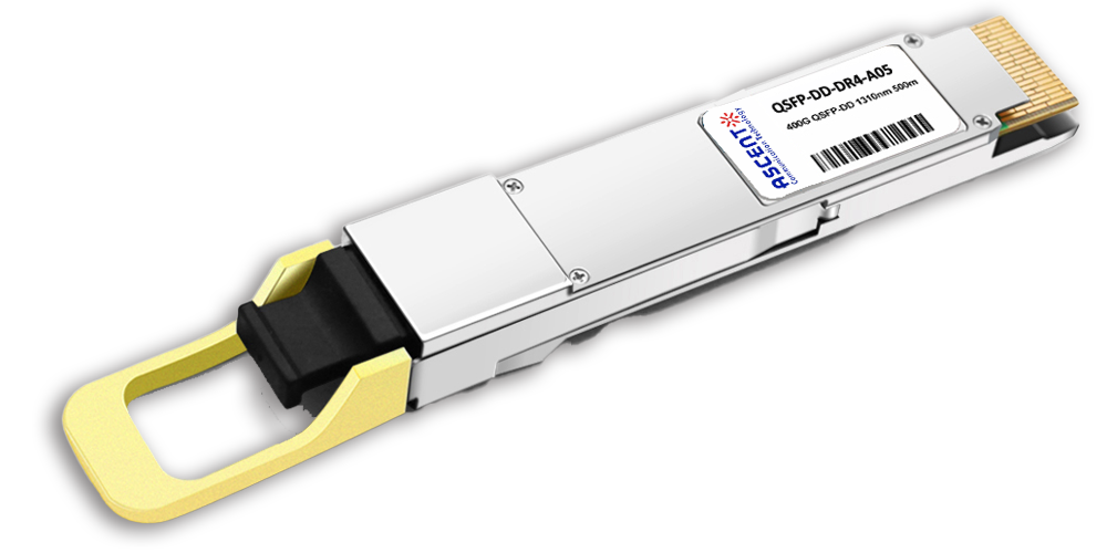
400G QSFP-DD DR4 500m
400 Gb/s QSFP-DD DR4 500m Transceiver
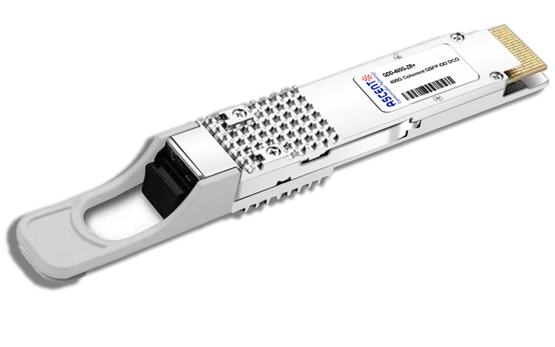
400G QSFP-DD DCO ZR
400G QSFP-DD DCO ZR Coherent Optical Transceiver
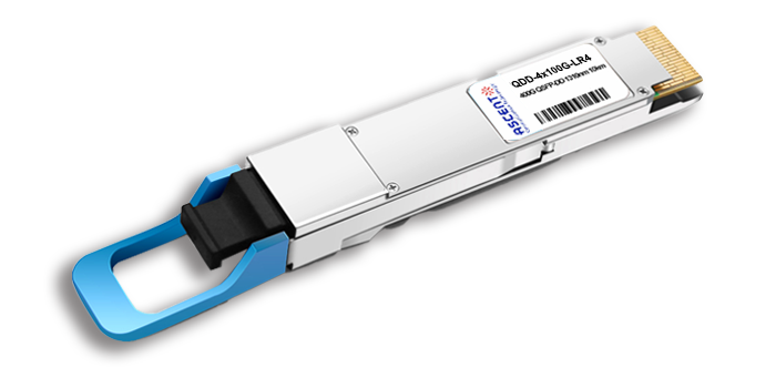
4X100G QSFP-DD LR4 10km
QDD 4x100G 1310nm LR 10 km Transceiver
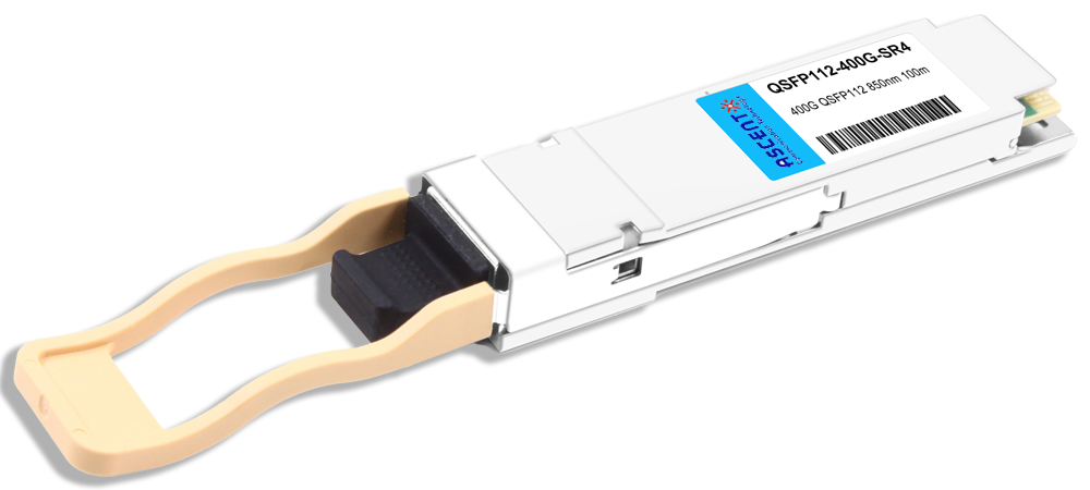
400G QSFP112 SR4 850 nm 100 m
QSFP112-400G-SR4-01 400 Gb/s QSFP112 SR4 850 nm 100 m Transceiver
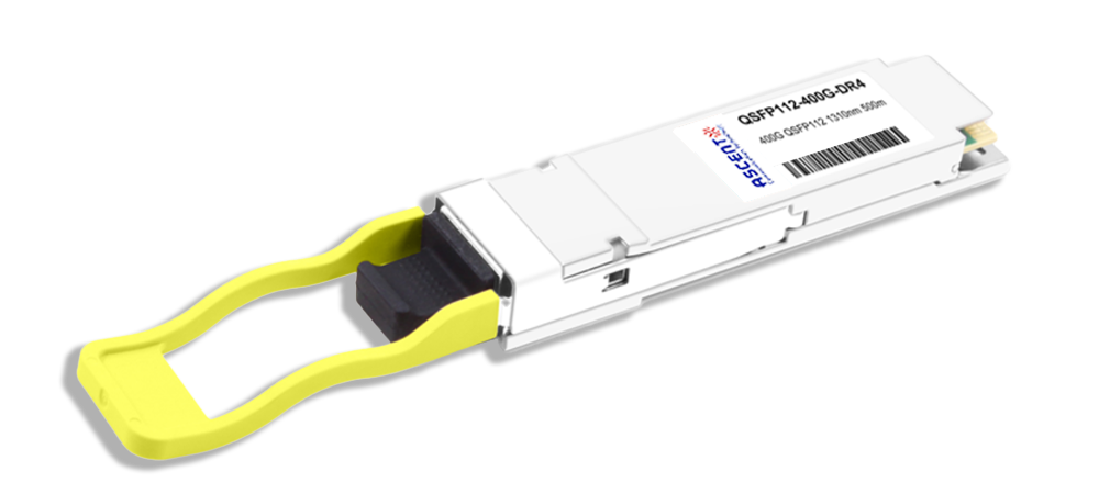
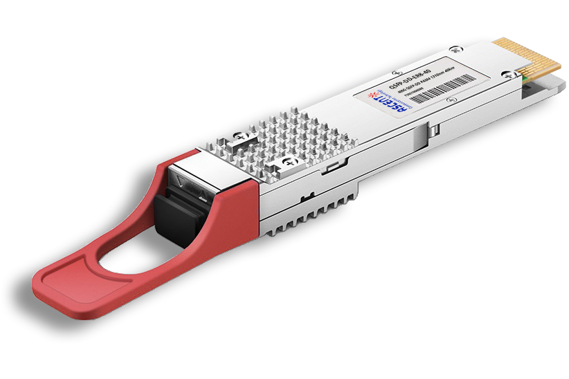
400G QSFP112 DR4 1310 nm 500 m
400G QSFP112 DR4 1310 nm Transceiver 500m
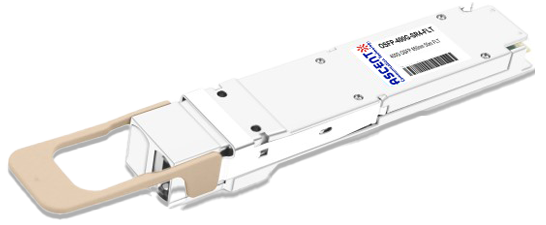
400G OSFP SR4 FLT 50m Transceiver
400 Gbps Multi-Mode 50m OSFP Transceiver
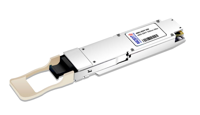
400G OSFP SR8 100m Transceiver
400 Gbps PSM8 Multi-Mode 100m OSFP Transceiver
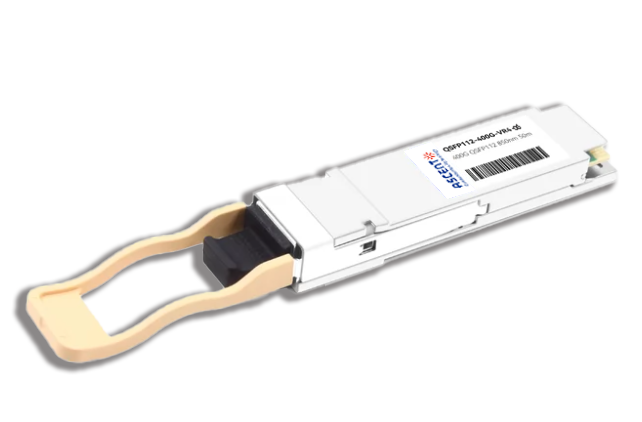
400G QSFP112 VR4 Transceiver
400G QSFP112 VR4
White Paper
Press Releases
Briefings 1
Briefings 2
Videos, etc.
QRG
Manual1
Manual2
Get in touch with our experts
Feedback